Hi everyone!
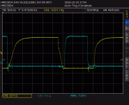
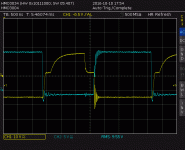
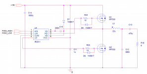
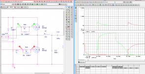
First of all forgive me, if opened an unnecessary thread, I am new to this forum. I want to design a class D audio amplifier using IR2011 gate driver. The PWM inputs are generated by a microcontoller (0-3.3V , 250 kHz, dead time: ~300ns which is already a lot). The schematic of the driver and the power stage are in the attachment diy_class_D. The problem I have is that the high side gate voltage doesn't reach zero fast enough during short pulses as it can be seen in attachments SCR029.gif, (yellow: high side, blue: low side) and it causes a shoot-through. In addition, the high side gate voltage goes up before there is even a input signal (notice the jump in voltage when the low side gate votlage goes low) However, when the high side gate voltage stays high longer, there is no such problem (SCR28.gif). Dead time is already very long, increasing it didnt help the problem. I am also simulating the circuit in PSPICE, it results are identical. (attachment diy_class_D_sim).
The design is currently on a prototype board. I know the IRF530 are not the best solution, so i already ordered a couple of IRFB4019 trenchfet technology mosfets. As I read on this forum, these should be just fine.
I hope you can help me, i would really appreciate it! Sorry if I didn't tell you any crucial information, just let me know if there is any.


You have to put two capacitors as close as possible to the ir, Vcc-Com 100-220 uf, Vs-Vb 10-22 uf low ESR in parallel with ceramic 100nf.
Why you use C13 at the output?
Increase gate resistor, 22-33 ohm are accettable value
Why you use C13 at the output?
Increase gate resistor, 22-33 ohm are accettable value
You have to put two capacitors as close as possible to the ir, Vcc-Com 100-220 uf, Vs-Vb 10-22 uf low ESR in parallel with ceramic 100nf.
Why you use C13 at the output?
Increase gate resistor, 22-33 ohm are accettable value
Thanks for the fast reply!
C13 removes the DC component of the output waveform, since the design has only one supply rail, and is referenced to ground.
I have already tried a lot of things, including a 22 uF cap paralell to the 220 nF booster cap. I also put more than enough capacitance right next to the IC, but I will experiment more with them.
The circuit is working actually, but this shoot-through creates a lot of distortion at the output, plus lowering the dead-time makes it worse.
The high side gate voltage doesn't have to reach 0 fast. It has to reach source voltage of high side FET (=Vs=half bridge output). No cross-conduction on the pictures.
Last edited:
What you can see on the first picture is a slow output transition and Zero Voltage Switching due to low ripple current and high output capacitance of the FETs.
At higher voltage this will be better due to decreasing Coss. A better FET also helps. Lower inductance also. And lower freq too.
At higher voltage this will be better due to decreasing Coss. A better FET also helps. Lower inductance also. And lower freq too.
Last edited:
Hi Pafi! (Szia Pafi)
Thanks for your feedback!
I meant the bridge voltage, not 0 V, sorry. Could you please specify what you mean by cross-conduction? (is it shoot-through)
I still don't understand why the gate voltage of the high side FET stops decreasing during short pulses.
What exactly do you mean by lower inductance? Lower the inductance of the output filter, or the stray inductances of the MOSFETs?
Hello Blase!
A MOSFET must be controlled by G-S voltage. The output voltage of a high side driver is this voltage, and not the voltage you measured between high side gate and gnd. The real output of the gate driver goes low fast, but despite the high side FET is now become turned off, Vs node can't go low immediately, because the D-S capacitance of high side FET must be charged to the rail voltage, and the low side FET's D-S capacitance must be discharged at the same time. This can be done ideally by the ripple current of output inductor, and if done this way then no loss is involved. If this current is too low, then the opening FET will do the rest of the job of charhing/discharging, but with power loss. This is still not a real shoot-through (=cross-conduction), but better to avoid if you can do without making other problem.
The reason why inductor current is low at that transition is not directly because of short impulse. It is affected by other factors also. The inductor current can be estimated by sum up load current and ripple current. Ripple current is a triangle wave with amplitude of Iripple_p=0.5*(Vpsu-Vout)*Thigh_pulse/L
I think I am starting to understand it, thanks for clearing it out for me! I will then try another inductor and try to measure the current flowing towards it. I wanted to design a PCB anyways, it might work better with a properly designed PCB.
Thanks again for your time and help!
Thanks again for your time and help!
Last edited:
Blase,
Youre welcome! You can try an other inductor, but there are more important things to do before. First of all finding a better measurement method. Looking at these 2 waveforms is not easy to understand what happens. You'd better measure low side gate and drain waveforms at once, and trust in symmetry (high side will behave the same way generally).
Now I see only 1 unusual thing: low side seems to be much faster than high side. This can be because of different gate resistors, or because you measure high side after the resistor but low side before resistor.
An other note: 18V is very low. If you really need this low voltage, then a lower voltage FET could perform much better. But if you need higher voltage, then at that voltage your current MOSFETs will be "faster" (lower output capacitance).
Is uC only a test device, or you want to use it in final design? There are strong quality limitations in uC, however there are techniques to overcome.
The simulated current waveforms are weird. Also the current probe symbol and especially the placement of them. You can't measure current inside a node. Current flows between nodes, on branches. When you place a current probe on a node, the program will select a branch nearby. In your case probably the resistor branch was selected. This because you can't see discharging current of the gates (diode bypasses this current). A correct simulation program only use current meters with 2 poles.
Periodicity. It's always good to know if the waveform is periodical or not. (And always simpler to analize a periodic waveform, so if it is possible to arrange a periodic operation that reflects the area of interest, than do it!) On your first picture the waveform is not periodic, but at least this can be seen. On the simulation result there is no information if it is periodic or not, the time slice is too short.
Pafi,
I am measuring the gate voltages directly at the MOSFETs pins, they both have 10 Ohm resistors in series. The circuit is working actually, but there is just a lot of distortion and noise on the output. I will post some measurement results about this tomorrow (with periodic signals as suggested).
After reading your comment yesterday I realised how much of a idiot I was, for not measuring the gate voltage referenced to the bridge voltage (Vs), so thank you again for your help!
I didn't intend to go higher with the supply voltage, since this circuit is mostly just a proof of concept, not a high power amplifier for home use.
The microcontroller is a STM32F407. I know that the quality won't even match an analog class D amplifiers quality, but I have already checked how fast it can modulate the input signal, and it is doing good up to 15 kHz. I am using DMA streams by the way, to change the duty cycle of the output signal. The ADC can sample the input signal at 500.000 kHz theoretically, but i haven't been able to check that.
I am using PSpice, as I know, this the one of the best circuit simulation programs out there. You can only place current probes at the pins of the device symbols. I attached a picture of the properly measured gate current.
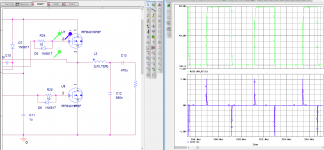

Be careful! Most oscilloscope have inputs with a single reference (gnd). Connecting it to the Vs node may cause a short circuit. You can display Vgs by subtracting Vs from Vg.
As you see on the simulation gate waveform should be much faster. I can't believe high side gate resistor was really 10 ohms. Measure it!
Distortion is caused by too much dead time, noise is probably the quantization noise. Not only PWM refresh rate is important. PWM quantization is also a weak point. And if ADC is not synchronised to PWM, then quality remains only a dream. In high level programming languages the high and variable latency makes high quality audio processing practically impossible. Maybe in assembly it is possible to provide fast and controlled timing.
For good quality with asynchronous resampling (this is what you do now) you must achieve a high oversampling rate.
Last edited:
I made the measurement exactly like you described it, since I don't have a differential probe.
I don't know why the the high side gate voltage rises so slowly, but i measured the gate resistor, and it's exactly 10,2 Ohm.
I didn't have time to make the measurements today unfortunately, I believe the bad ground connections also factor into the noise/distortion problem.
I indeed try to oversample the input signal. As for quantization, I have 335 different duty cycle levels, which is not a lot, but I can increase it to 670 and still have a 250 kHz PWM. Other option is to lower the frequency. The uC modulation is still under development, it is yet to be seen, how much I can get out of the STM32F4.
Can you show the circuit built?
Vcc is quite high if really 18V. Maybe IC fried.
The proper PWM resolution for quality audio is 100 times more at least. You need dither, with 2nd order noise shaping. But for first time a simple integrating feedback would do well.
Vcc is quite high if really 18V. Maybe IC fried.
The proper PWM resolution for quality audio is 100 times more at least. You need dither, with 2nd order noise shaping. But for first time a simple integrating feedback would do well.
I won't be able to squeeze out more of the uC, so it will have to do. Again, this is mostly just a proof of concept, that you can use digital signal processing for audio amplifier.
The circuit is working, the IC is fine. I am planning to use feedback to improve the circuit.
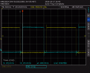
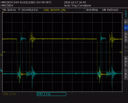
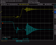
Attachment SCR01.gif shows the uCs PWM outputs without VCC applied to the circuit. SCR03.gif shows it with VCC applied. Lots of ringing there, also SCR08 shows that the amplitude of the ringing is very high. I guess my connections on the prototype board have lots of stray inductances.
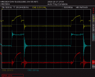
SCR07 shows the properly measured high side gate voltage (red signal), and the output of the transistors (blue).
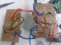
I also attached a picture of the circuit, I know it's a mess, sorry about that, I am not very good at making prototype circuits. I am still planning to design a PCB, I think it would help.
Thank you again for your help, I really appreciate it. I think I owe you a beer, or two at this point.


- Status
- Not open for further replies.
- Home
- Amplifiers
- Class D
- IR2011 High side gate voltage problem