After building several power amps with Lateral outputs, I became aware of the difficulties and determined some best practices on how to implement these OPS.
This new amp (the Assemblage VIII) has this name inspired by the mix of grapes used to make some very special wines in Switzerland.
As the name implies, once again I use several techniques I learned while reading about Lateral power amps in diyaudio.
Now in simulation stage, It will become reality once I get enough proof of feasibility.
As usual I will post my findings here hoping to rise the interest of the specialists.
Here you have the schematic and some files to play with LTSpice:
Attachments
Last edited:
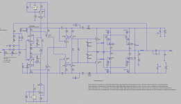
Now that I have a working simulation I will analyse the circuit.
Input transistors bases are connected together and referenced to GND so biasing is done by the ccs that feed the emitters of the input bgt.
Feedback from the output is injected directly in the input.
Voltage divider R5 and R4 defines quantity, C3 isolates the circuit for DC and the current limiting R6 (18k) is bypassed by the compensation capacitor.
I set R4 to 400ohm so to have 26dB gain (closed loop).
IPS transistors are wired as common emitters so they provide voltage amplification with phase inversion. Gain is set by the ratio between collector and emitter resistors (R7 and R8 in the positive side).
For the positive side Q1, amplified signal comes from the collector that enters the base of Q3 (another common emitter).
Then follows a cascode Q6 that feeds the mirror responsible by transmiting the current to the voltage spreader that sets bias on the OPS. (Voltage spreader is purely resistive).
The OPS uses medium power bjt for driving the output lateral mosfets.
R1 + R2 set input impedance and R1 C2 form a low pass input filter.
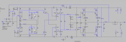
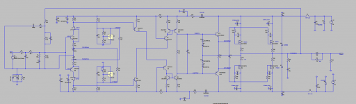
Although it sims well, this circuit is too complex.
The external ccs are needed to create a voltage (+-5V) on top of the resistors R12 and R16.
So I removed the ccs and loading resistors R10 and R15 and replaced them by two voltage sources around two TL431 references.
I also needed a current production jfet pair for the IPS cascodes (2N5486 2N5462 are very difficult to get) so I am now using J113 NFet and J176 PFet.
Last edited:
- Status
- Not open for further replies.
- Home
- Amplifiers
- Solid State
- Inverting topology power amp (Assemblage VIII)