Hi,
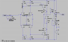
I made a sketch for an openloop stage with ~30dB gain.
Sim only, for the moment.
This is how it works (at least, how I understand it does...):
The heart of it is complementary version of a grounded gate diff-amp with 'no' miller effect (or it would be with R1/R8 = 0).
The cascoding FET's (J4/J8) shouldn't show a miller effect as well, but without Q1/Q2, high-Freq rolloff starts very early at only some Khz. With Q1/Q2 present, it's no earlier than 70Khz (see next posting).
FET models sim a IDSS of 14.8mA, so I real world biasing would show different values for some parts.
J6 is present for convenience in the real world when finding the optimum base voltage for Q1/Q2.
This cascode connection has been used by borbely, curl, pass and many others, it is discussed in the A75 article and in the new borbely-papers, for instance. There is a patent of M.Noro which goes into details as well (all infos at diyaudio.com 🙂
Because the circuit depends strongly from any load, it needs buffering.
I'm looking forward to build it.
Unfourtunatly, I don't know how to perform square-wave tests oder distortion measurement in LTSPice to look for fundamental errors.
A few questions:
-Why is miller effect still present at J4/J8?
-How to calculate the optimum load (R12)?
- How can I adjust the fet models, so I can set them to my real world devices (a bunch of 2sk389/2sj109 around 6-9 mA IDSS)?
thanks,
Rüdiger
Attachments

I build the real circuit (without output follower), and while the sim with LTSPice showed wildly different dB-numbers for very near values of Rl, the real circuit is much more robust against loadchanges.
If all fits, it shall drive the 50/500 pole of a riaa network.
At 23.5dB, it puts out fine waveforms (no distortion measurement gear at my command, sadly), a 20 Khz square wave is, well, square.
Sadly, I have too few V-grade FET's. I guess it's best to switch for beefier parts for the cascode, with my 11mA IDSS parts I have to go down to 2.5mA for the input pairs to get best waveforms.
Rüdiger
Hi,
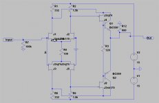
now I build the attached circuit. Other than indicated, the input pair are 2sk389/2sj109 with an IDSS around 7mA running at 6mA. The cascode fet's take 11mA, the bjt's take 9.
The ouput sits at 300mV DC at the moment, gain is 100. The square looks perfect till 70Khz and slowly rounds till it loses gain at perhaps 300Khz.
It is perfectly stable, power on and off are very smooth.
Can't wait to actually hear it.
Rüdiger
Attachments
Hi
It appears to me that the input capacitance of the j-fet is much greater than that of the BJT. The input impeadance of the BJT may be lower at 0Hz because of base current but it is more resistive, so when viewing higher frequencies like in that 70KHz SW, the input capacitance of the j-fet used as the gain stage loads the input differentials more, reducing dV/dT. Try using the BJT's as the gain stage and the j-fet's as followers. R3 could be eliminated since the j-fet follower is self bias, with source resistors. This way the BJT's, with a lower impeadance, are driving the j-fet input capacitance instead of the input stage. Also you could try BJT's for the gain stage and follower. Might have to adjust R1,2,8,9 a bit though but I would be interested in the simulation results to see if it is faster.🙂

It appears to me that the input capacitance of the j-fet is much greater than that of the BJT. The input impeadance of the BJT may be lower at 0Hz because of base current but it is more resistive, so when viewing higher frequencies like in that 70KHz SW, the input capacitance of the j-fet used as the gain stage loads the input differentials more, reducing dV/dT. Try using the BJT's as the gain stage and the j-fet's as followers. R3 could be eliminated since the j-fet follower is self bias, with source resistors. This way the BJT's, with a lower impeadance, are driving the j-fet input capacitance instead of the input stage. Also you could try BJT's for the gain stage and follower. Might have to adjust R1,2,8,9 a bit though but I would be interested in the simulation results to see if it is faster.🙂
Onvinyl said:sorry, bjts sit at 12mA
You really need some emitter degeneration here to define the quiescent current through the BJT's. I'm actually surprised that you haven't smoked them yet. Consider ~10 ohms on each emitter and perhaps even replacing R3 with a series pair of 1N4148’s or similar.
Cheers,
Glen
G.Kleinschmidt said:
You really need some emitter degeneration here to define the quiescent current through the BJT's. I'm actually surprised that you haven't smoked them yet. Consider ~10 ohms on each emitter and perhaps even replacing R3 with a series pair of 1N4148’s or similar.
Cheers,
Glen
Well, I *did* smoke them, when I made R3 too large...
I will try all suggestions as soon I have the time!
Rüdiger
edit: yes, I did try it with two bjt's, it *is* faster but it gave me some problems that looked like ringing. I will investigate further.
It looks like R1/R8 degenerate J4/J8, the question is, to what degree? Some degeneration on Q1/Q2 is still a good idea.
The case is different if you use fets or bjts in the fc-position.
As shown, the cascode fet's take 11mA. If you omit R3, almost all the current flows through the fet, by enlarging R3's value you balance the current between bjt and fet.
Q1/Q2 don't seem to need any degeneration.
It's not easy to predict the DC behavior without sim (or build) because of the interdepency of the biasing. The voltages that appear over R1/R2 set the Vgs of the fet which sets Id which in turn changes the voltage drop over R1. The DC-behaviour is stable, however. If you change R1 you change, of course, the net current of J4/Q1, by adjusting the value of R3 you split the current between the two. I couldn't see much difference in the output-waveforms for any reasonable current split. Will see later, if it changes sound.
I made a quick sim, with interchanged fets and bjts in the cascode, R3 can indeed omitted and it indeed has better shaped sqw and extd. bandwith.
I'm running out of time however, I will try the interchanged design in a few days on the workbench.
Rüdiger
Onvinyl said:The case is different if you use fets or bjts in the fc-position.
As shown, the cascode fet's take 11mA. If you omit R3, almost all the current flows through the fet, by enlarging R3's value you balance the current between bjt and fet.
Q1/Q2 don't seem to need any degeneration.
It's not easy to predict the DC behavior without sim (or build) because of the interdepency of the biasing. The voltages that appear over R1/R2 set the Vgs of the fet which sets Id which in turn changes the voltage drop over R1. The DC-behaviour is stable, however. If you change R1 you change, of course, the net current of J4/Q1, by adjusting the value of R3 you split the current between the two. I couldn't see much difference in the output-waveforms for any reasonable current split. Will see later, if it changes sound.
I made a quick sim, with interchanged fets and bjts in the cascode, R3 can indeed omitted and it indeed has better shaped sqw and extd. bandwith.
I'm running out of time however, I will try the interchanged design in a few days on the workbench.
Rüdiger
Ok, having a closer look at you circuit this time, I see that the collectors of Q1 and Q2 return to the JFET sources to make a kind of symmetrical CFP.
My previous post can be disregarded.
Cheers,
Glen
The circuit runs most smoothly when keeping the fets in the folded cascode position (with added resistance between both drains) then driving mosfets (instead of BC550/560). I could even drive my headphones with it (okay, this steels some gain) when I used irf610/9610. With shunt regs running at +/- 24V it sounds real promising!
Rüdiger
Rüdiger
Hi lumanauw,
still, it is not a final design.
The DC-workingconditions seem stable.
The output sits at 300mV yet, and is dependent of the load that is presented to its output. As is the gain and linearity (transconductance amplifier).
The output mosfets are not matched yet (the other fets are), so it will maybe better in the end. It will need a servo, I think.
One could fineadjust R9, for instance, but that corrupts AC-behaviour according to the sim.
More ideas are welcome.
Rüdiger
Hi,
inverting was not the primary goal. The idea was to use the diff pair in a 'no-miller', or perhaps, less-miller mode. See first posting.
Rüdiger
inverting was not the primary goal. The idea was to use the diff pair in a 'no-miller', or perhaps, less-miller mode. See first posting.
Rüdiger
Hi,
it is inverting as shown.
Swap the inputs and it becomes non-inverting?
Any downside?
Since there is no GNFB, the two inputs are identical making it very worthwhile taking both to the input plug and grounding the unused input at the input socket.
Even better, use an XLR and two core and take the unused input all the way back to the source unit and ground it inside the source.
Heck, go fully balanced.
Hi Rüdiger,
Have you finished the other input stage yet?
For the second time in just two weeks: nonlinearities in JFETs are basically caused by varying, high parasitic capacitances which can be effectively reduced by keeping Vds constant. Limiting their operating area at the same time is important too. Cascoding can provide that and several other advantages, when applied properly. It is no the case in your design so do not expect much.-Why is miller effect still present at J4/J8?
Have you finished the other input stage yet?
AndrewT said:Hi,
it is inverting as shown.
Swap the inputs and it becomes non-inverting?
Any downside?
Since there is no GNFB, the two inputs are identical making it very worthwhile taking both to the input plug and grounding the unused input at the input socket.
Even better, use an XLR and two core and take the unused input all the way back to the source unit and ground it inside the source.
Heck, go fully balanced.
Hi Andrew,
if I swap the inputs, the bandwith suffers. Again, AoE, where they discuss the miller effect.
Yes, the balanced option springs in one's face, but I'd lose the non-miller benefit.
It's intended for as the second stage in a phonoamp which does not go balanced. A balanced circuit could be made, as is thoroughly discussed in the blowtorch thread.
Hi Lumba,
we have a variation of the folded cascode here. Further cascoding of the input pairs as well as the FC-pair yields no benefit, according to all the things I tried.
My input stage waits till I matched some fets. Matching is ... boring.
Rüdiger
- Status
- Not open for further replies.
- Home
- Amplifiers
- Solid State
- Inverting FET openloop gainstage