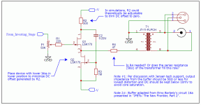
I’ve been exploring (in simulation world) the use of a line output transformer to correct the phase inversion of the H2 and B1K circuits. If the H2 / B1K are configured as unity gain buffers, a switch, relay and logic gate could also be added to allow the H2 / B1K to be toggled in and out of the circuit as desired with absolute polarity on the output true to the source. The transformer would be added after the H2 / B1K circuits and would provide the added benefits of galvanic isolation and balanced outputs.
I contacted Jensen tech support and they recommended the JT-11-FL / JT-11-FLPCH for this application. They indicated that for optimal performance, the output impedance of the stage driving the transformer should be 50 Ω or less and DC offset should be 10 mV or less to avoid core saturation. A consequence of output impedance requirement is that an AC coupled topology would need an excessively large coupling cap to maintain a decent frequency response. Therefore a low-impedance, DC coupled buffer with near zero DC offset is needed to drive the transformer.
The H2 and B1K output stages are AC coupled with output impedances of 150 Ω+. An additional buffer is needed to drive the transformer. This would also allow the main volume control to be added after the H2 / B1K if you’d like to maintain the “ideal” 1.0 V of signal across the output of these circuits.
In LT Spice simulations, a “Mezmerize B1” buffer has decent output impedance if the series output resistor is eliminated, but the distortion performance isn’t great. I tried Erno Borbely’s version of this circuit (Figure 16a in his JFETs: The New Frontier, Part 2 article) and the distortion performance improved significantly (0.2% to 0.01% at 1kH).
A note on simulations – LT Spice is usually overly optimistic on distortion and my modeling of a Jensen output transformer is likely not great. As a result, I’m not interested in the absolute numbers, but instead the relative difference between the two circuits. I’d like to hear some opinions on if this is a valid approach.
The circuit attached has a slight modification to Erno Borbely’s design. The 22 Ω resistor at the source of the current source has been removed. I believe this was added to make the circuit more linear, but its presence causes DC offset at the output.
I have a few questions on it:
- Is the series output resistor R4 needed or would the series resistance of the output transformer suffice? Assuming the ability to drive capacitive loads is a requirement. If you plan to connect this to the following stage with a short cable, maybe R4 is irrelevant?
- The modeling in LT Spice suggests DC offset of 1 to 4 mV with the JFETs matched to within 0.1 mA. Is this likely in the actual physical circuit?
- The modeling in LT Spice suggests that DC offset can be reduced further by placing the lower Idss device in the current source position (assuming a 0.1 mA mismatch) and then making R2 a trimmer (a lower Idss current source generates positive offset and R2 generates negative offset). Is this a realistic approach in a real circuit? Or would the temperature dependent nature of the JFET make this difficult to implement in practice?
- If 1.0 V rms is the maximum expected signal, then I assume a lower supply voltage could be used than the ±24 V specified in the Borbely article. However the ±24 V is a beneficial as it would allow the positive side of the supply to power the H2 or B1K if they are implemented in the same chassis (assuming the supply can handle load imbalances). Keeping the Idss of the JFET down would keep dissipation down. My models for the LSK170 have an Idss of 8.5 mA which results in about 210 mW of dissipation. What value of Idss would a circuit like this need? I had 6 mA in mind – I believe this is what the Erno Borbely circuit ran at. Maybe is can run effectively on lower Idss devices considering an expected 1 Vrms source?
Attachments
If you are going to add another stage why don’t you just choose one that is inverting? Problem solved, no need for a transformer.
Unless you really like transformers. In that case, redesign the jfet buffer after the nutube for lower R out. MOSFET will work. Adding another stage is so you can add a transformer doesn’t make a lot of sense in my opinion.
Unless you really like transformers. In that case, redesign the jfet buffer after the nutube for lower R out. MOSFET will work. Adding another stage is so you can add a transformer doesn’t make a lot of sense in my opinion.
To stay with the theme of the H2 & B1K, I’d prefer to avoid op amps, excessive NFB and overly complicated designs. It also needs to be DC coupled to avoid a 470+ µF coupling cap. I’ve had trouble finding a discrete inverting design that meets these criteria. I’m open for any suggestions.
I’m also not clear on how you could redesign the existing H2 or B1K circuits to provide a low-impedance, DC coupled output with near zero DC offset. The H2’s SE common source configuration would require some type of level shifter to address the DC but would still likely have too high of an output impedance to drive a transformer. You might be able to tweak the B1K to make it work. Seems simpler to just add an output buffer as I suggested. Then it could also be used with the H2 and allows the volume to be placed after the H2/B1K stage.
I’m also not clear on how you could redesign the existing H2 or B1K circuits to provide a low-impedance, DC coupled output with near zero DC offset. The H2’s SE common source configuration would require some type of level shifter to address the DC but would still likely have too high of an output impedance to drive a transformer. You might be able to tweak the B1K to make it work. Seems simpler to just add an output buffer as I suggested. Then it could also be used with the H2 and allows the volume to be placed after the H2/B1K stage.
To stay with the theme of the H2 & B1K, I’d prefer to avoid op amps, excessive NFB and overly complicated designs. It also needs to be DC coupled to avoid a 470+ µF coupling cap. I’ve had trouble finding a discrete inverting design that meets these criteria. I’m open for any suggestions.
I’m also not clear on how you could redesign the existing H2 or B1K circuits to provide a low-impedance, DC coupled output with near zero DC offset. The H2’s SE common source configuration would require some type of level shifter to address the DC but would still likely have too high of an output impedance to drive a transformer. You might be able to tweak the B1K to make it work. Seems simpler to just add an output buffer as I suggested. Then it could also be used with the H2 and allows the volume to be placed after the H2/B1K stage.
Hello brian92fs.
There's a possible solution regarding your bolded statement above.
1. The Pass-suggested quiescent [DC] conditions of the H2's special FETs are untouchable.
2. Use the complementary JFETs by Linear Systems [LSK/LSJ] to interface between the capacitor-coupled output of H2, and the downstream device. This buffer has a low output impedance. A dual voltage PSU is needed. diyF5 and diy F6 use this buffer.
Best
Anton
I've looked at that design. It's discussed in figure 16b of the Erno Borbely article I linked to above. It's output impedance is higher than the circuit I suggested (though still under 50 Ω) and the distortion performance in simulations isn't as good (about 5x higher).
However, since simulations aren't reality, it would be a good candidate for testing.
However, since simulations aren't reality, it would be a good candidate for testing.
I've looked at that design. It's discussed in figure 16b of the Erno Borbely article I linked to above. It's output impedance is higher than the circuit I suggested (though still under 50 Ω) and the distortion performance in simulations isn't as good (about 5x higher).
However, since simulations aren't reality, it would be a good candidate for testing.
You are searching for a buffer which inverts phase by 180 degrees; say for the output of H2. If by this example the equipment after H2 [preamp, power amp] does not invert phase, then you can easily invert overall phase acoustically by reversing the leads of the loudspeakers. An application usually suggested by Mr. Pass. No need for another electronic device in the signal stream.
BUT note; when you invert the phase of H2's output either electronically with an inverting buffer or acoustically, THEN you have switched the performance of H2 from H2 negative phase [H2np] to H2 positive phase [[H2pp].
Please see the thread in the Pass Labs Form by DIYer juma which is entitled LSK pre-BAF 2013. It works as a buffer which inverts phase.
Best
Anton
Hi Anton, I’m aware of NPs recommended approach for swapping the speaker leads on the H2/B1K. However, it doesn’t help with my two goals.
It’s also fun trying to design a solution to accomplish this. 🙂
Thanks for the thread reference. I’ll look it up.
- I’d like to be able to toggle the H2/B1K in and out of the signal chain while maintaining the polarity at the outputs.
- I’d also like the ability to toggle between positive and negative H2 harmonics by toggling polarity on the outputs.
It’s also fun trying to design a solution to accomplish this. 🙂
Thanks for the thread reference. I’ll look it up.
Please see the thread in the Pass Labs Form by DIYer juma which is entitled LSK pre-BAF 2013. It works as a buffer which inverts phase.
Thanks again for the reference. For those interested it's here: LSK pre - BAF 2013
Interesting read. If you wanted to pass the "ideal" 1V across the H2 or B1K, you could follow it with a version of those preamps to correct the polarity and provide 10 dB or so of gain to drive a F5 or F6.
I am not so convinced 1V is "ideal". I think it might just be the point of reference that Nelson is using for measurement.
I agree. Hence the use of quotes. Though there probably is an ideal level for each specific build and listener preference.
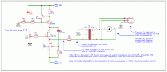
The shield on your RCA socket, which normally is at chassis potential, connects to the “cold” pin 3 of your XLR. Pin 1 of the RCA, the shield, should not be connected to the transformer (pin 8) at all.
The shield on your RCA socket, which normally is at chassis potential, connects to the “cold” pin 3 of your XLR.
I don't follow... I'm looking at my schematic in post #1 and don't see this connection.
Pin 1 of the RCA, the shield, should not be connected to the transformer (pin 8) at all.
I'm following the recommendations from Jensen. For example, refer to their Application Note Interconnection of Balanced and Unbalanced Equipment. It appears to show the unbalanced outputs connected in the manner I have depicted.
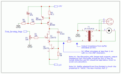
A little more tinkering with this. Replacing resistor R2 with an active current source eliminates the DC offset that R2 creates. It also appears to reduce distortion further, though seems to be very sensitive to tuning to a specific value (in simulations at least).
Attachments
I thought the connector below the XLR symbol was a RCA socket. If it is planned to float with regard to chassis and ground, OK, but you have to consider the unbalanced cable going to the connected equipment (power amplifier presumably) and the screen of this bringing its ground into your H2. If you use XLR and RCA simultaneously this will interfere with the balanced operation. If you only connect one at a time it might actually be OK, provided the RCA is not directly screwed into the chassis or otherwise having some connection to GND.
Please also refer to their figure “Typical Unbalanced Output” and the connection of the RCA to chassis and signal grounds.
I thought the connector below the XLR symbol was a RCA socket. If it is planned to float with regard to chassis and ground, OK, but you have to consider the unbalanced cable going to the connected equipment (power amplifier presumably) and the screen of this bringing its ground into your H2. If you use XLR and RCA simultaneously this will interfere with the balanced operation. If you only connect one at a time it might actually be OK, provided the RCA is not directly screwed into the chassis or otherwise having some connection to GND.
The output connectors do represent a XLR and RCA connector. The intent is to allow for either a balanced or unbalanced output. But not both simultaneously. The RCA is intentionally left floating for galvanic isolation. This configuration is described in figure 32 of Audio Transformers – Bill Whitlock Chapter 11 from Jensen's website. This also shows the addition of ferrite beads and clamping diodes - not sure if these should be added to this design.
In the Datasheet of the JT-11 XLR-Pin 1 connects to Chassis not Ground.
You are correct. My schematic was a bit oversimplified in that respect. Corrected schematic attached. Thanks for catching this.
Please also refer to their figure “Typical Unbalanced Output” and the connection of the RCA to chassis and signal grounds.
The figure you referenced is for an output driven from an opamp without an output transformer. I don't believe it applies to this implementation. If you look through the numerous schematics form Jensen, the RCA outputs are often depicted as floating for galvanic isolation.
Attachments
Last edited:
The output connectors do represent a XLR and RCA connector. The intent is to allow for either a balanced or unbalanced output. But not both simultaneously. The RCA is intentionally left floating for galvanic isolation. This configuration is described in figure 32 of Audio Transformers – Bill Whitlock Chapter 11 from Jensen's website. This also shows the addition of ferrite beads and clamping diodes - not sure if these should be added to this design.
Well, you have the situation under control!

My main concern was not being able to use RCA and XLR at the same time, which is seldom necessary.
You are correct. My schematic was a bit oversimplified in that respect. Corrected schematic attached. Thanks for catching this.
The figure you referenced is for an output driven from an opamp without an output transformer. I don't believe it applies to this implementation. If you look through the numerous schematics form Jensen, the RCA outputs are often depicted as floating for galvanic isolation.
Yes, sorry, I was too quick on that one.
Good luck with the rest. 🙂
Last edited:
- Home
- Amplifiers
- Pass Labs
- Inverting buffer for H2/B1K