I hope it is something different, really can not read about all good ideas here. Instrumentation amplifier is very stabile way for handling amp inputs, and with some modifications could be used as additional gain source used for negative feedback. If assembled of two similar opamps with similar phase shift, simulators shows that it is easy to compensate circuit only with adjusting c2 and c3 on attached schematic. U1 and U2 shows err correction circuit with U4 (which should act as gainclone together with q1...q4) embedded in feedback loop. As gainclones can sound as serious amplifiers I expect this modification to make them even better. Every suggestion is welcome, hope I'll succeed with prototype to show you results 🙂.
Attachments
Quite a novel use of a "spare" op amp as an error amplifier. There are few things I'd consider.
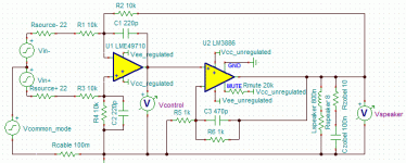
In fairness, the balanced composite chipamp approach does have its limitations. In most cases 0.1% resistors and 1% caps around the difference amplifier suffice to hold CMRR to 45dB or better given a balanced source using 1% resistors and a decent layout---the worse cases occur at the RC corner frequency well above the mains harmonics of the ground offset between the power amp and its source. Unless one has funky mains wiring, grounding issues, or level management problems this is usually good enough. For an unbalanced source Rsource- is just the ground resistance, meaning R1 in the schematic I've attached wants shimming by whatever Rsource+ happens to be. That's not commerically viable but it's often easy enough in DIY.
- Given a good choice of U4 an op amp driving a discrete power stage will outperform chipamps due to the op amp's higher GBP. At 6.5MHz typ the LT1055's not a bad approximation of the 5-8MHz typ GBP of chipamps, so the schematic here is well posed in that regard (though instances of R8 are needed on both emitters to avoid thermal runaway and R9 is on the small side by around four orders of magnitude). However, one can trivally swap the LT1055 for a more performant part such as an LME49710, which largely obviates the need for error correction. A single op amp circuit like this pairs well with darlingtons such as the Sanken STD03N and STD03P for a simpler build and better thermal tracking of the bias. Also, consider generating the bias from a current source such as the LM334 for reduced supply interaction.
- Rather than a discrete build of the power stage it's easier to use a chipamp such as the LM1875 or LM3886. Error correction of these parts by adding a controlling op amp to form a composite amplifier is pretty straightforward. Such designs are often referred to as nested feedback chipamps on this forum and, like the design proposed here, are often implemented with unbalanced inputs. Unbalanced implementations suffer from a problem, however. Chipamp THD is generally around 0.1%, meaning output voltage errors on the order of 100uV for typical home audio listening levels of a few hundred mV. 100uV is the same range as typical common mode offsets between a power amplifier and its source. Since unbalanced inputs have 0dB of common mode rejection this means the circuit's only addressing about half of the total error.
- Balanced composite amplifier implementations provide common mode rejection as well as chipamp error correction, with the residual error generally being dominated by the CMRR limit imposed by source impedance matching. A basic implementation of this topology is shown in the schematic I'm attaching to this post (feedback resistors and caps are starting points, note use of a more performant op amp than the LT318A for greater error correction). U1 should look familiar as it's a difference amplifier and fills the same role as the difference amplifier U4 in post 1's schematic. If one requires a higher input impedance or lower noise the usual two op amp front end of a three op amp instrumentation amplifier can be placed before the difference amplifier as usual. From an error reduction standpoint it's more useful to increase the common mode input impedance, making a THAT 1200 probably the most attractive frontend choice.
In fairness, the balanced composite chipamp approach does have its limitations. In most cases 0.1% resistors and 1% caps around the difference amplifier suffice to hold CMRR to 45dB or better given a balanced source using 1% resistors and a decent layout---the worse cases occur at the RC corner frequency well above the mains harmonics of the ground offset between the power amp and its source. Unless one has funky mains wiring, grounding issues, or level management problems this is usually good enough. For an unbalanced source Rsource- is just the ground resistance, meaning R1 in the schematic I've attached wants shimming by whatever Rsource+ happens to be. That's not commerically viable but it's often easy enough in DIY.
Attachments
Quite a novel use of a "spare" op amp as an error amplifier. There are few things I'd consider...
Hello, thank you for reply. I have to say that main idea with this topology is invented for driving differential amplifier, precisely for lowering Re, increasing gain and increasing input impedance of course. This schematic (post 1) is very optional, only for marking idea, and I can see that some values stayed as used for test only (c2 and c3 should be much lower), by mistake. I will provide real schematic if prototype justify expectations. So, yes, idea here is to use it with lm3886 or tda729x. But there is no such model in ltspice, and if I made it somehow it will not be as accurate as real build and I chose second. In the end, it is all about sound. I like stability of that concept, but I don't know will it improve or ruin sound quality. So I have to build it to hear how it sounds. After all, it is not complicated and it is fun 🙂. When done with my work you will be informed for sure.
Regards!
After few hours, character still changing. But already speakers and amp disappeared, I really enjoyed music last hours. Never suppose that gainclones can be so enjoyable.
- Status
- Not open for further replies.