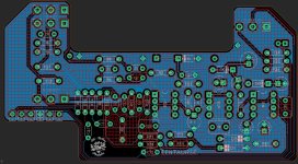
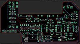
I’ve been reviewing several posts, but must of all address complex PCB design 4 layers whilst others address self etched ones. I’m looking for the most common do's and don'ts on PCB design I’m uploading an example on one of the latest PCB's designed, I thought I was doing ok, avoiding to cross traces from one side another. Also avoiding vias and keeping things tidy. Now I know I’m supposed to do thicker traces over 20mil instead of the 6mil I was doing. Also the top plane is hatched with VR just because I like how it looks, but apart from being unnecessary to hatch it, it might also do wrong in the design the bottom plane is solid GND. I also know power traces must be cross on a 90° angle. In this example there are no power crossings just one sole signal crossing, also I go in between DIP holes with some traces, I guess I should avoid those as well, please let me know. What are your suggestions on what would you do to improve this design cause it tends to get noisy due to the charge pump IC