I am facing this problem, which is causing the two push-pull MOSFET to extreme stresses.
I am using this to power TAS5630 amp. the boost converter is converting the 12V DC voltage to 36V DC (unregulated). As this is a car amplifier so the battery voltage can be 10V to 14.5V.
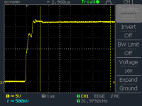
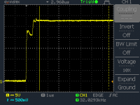
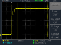
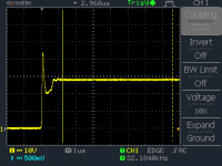
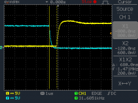
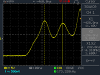
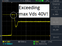
Everything is ok upto 13.5V DC input. But when the input voltage is higher than that, inductive spike is seen at the MOSFET drain and they becomes hot.
At 13.8V or higher the kick exceeds the max Vds 40V and the FETs are starting to runaway.
I have attached some screenshot and unsnubbed oscillation at MOSFET drain. Please help me to remove the inductive kick @15V.
I am using this to power TAS5630 amp. the boost converter is converting the 12V DC voltage to 36V DC (unregulated). As this is a car amplifier so the battery voltage can be 10V to 14.5V.
Everything is ok upto 13.5V DC input. But when the input voltage is higher than that, inductive spike is seen at the MOSFET drain and they becomes hot.
At 13.8V or higher the kick exceeds the max Vds 40V and the FETs are starting to runaway.
I have attached some screenshot and unsnubbed oscillation at MOSFET drain. Please help me to remove the inductive kick @15V.
Attachments
-
 0drain-gnd1 @13.5V.png2.5 KB · Views: 206
 -
 0drain-gnd1 @13.8V.png2.5 KB · Views: 204
 -
 0drain-gnd1 @13.9V.png2.5 KB · Views: 190
 -
 0drain-gnd1 @14.0V.png2.4 KB · Views: 200
 -
 0drain-gnd1 @14.2V.png2.6 KB · Views: 200
 -
 Dead zone.png2.8 KB · Views: 64
 -
 Adrain-gnd2 @12.0V Unsnabbed.png3.4 KB · Views: 74
 -
 Adrain-gnd1 @12.0V Unsnubbed.png3.3 KB · Views: 75
 -
 0drain-gnd1 @14.5V2.png8.1 KB · Views: 76
 -
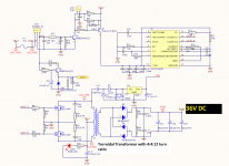 schematic.png208.1 KB · Views: 134
Last edited:
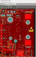
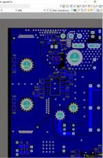
Picture of layout?
Here is the top and bottom layout.
Attachments
Sorry for the expression, but boosting to >36V with such an unstable (by its very nature) voltage source and using *just* 40V rated parts, is suicidal.
There's a concept called "safety margin" which you are ignoring, at your risk.
1) use *at least* parts rated 60V , period.
There's some parameters you can NOT tweak, one of them is avalanche voltage, it's built in at the Factory.
2) that said, I agree that it's good to attenuate ringing and peaks, within reason of course.
Properly dimensioned snubbers and some Zener will help you.
Sorry for the expression, but boosting to >36V with such an unstable (by its very nature) voltage source and using *just* 40V rated parts, is suicidal.
There's a concept called "safety margin" which you are ignoring, at your risk.
1) use *at least* parts rated 60V , period.
There's some parameters you can NOT tweak, one of them is avalanche voltage, it's built in at the Factory.
2) that said, I agree that it's good to attenuate ringing and peaks, within reason of course.
Properly dimensioned snubbers and some Zener will help you.
The MOSFETs are rated as 40V where the max voltage should be (without spike) around 28V. These are for primary. The secondary has 36V, where no MOSFET is present. Is not it enough safety margin ?
40 V is enough. Inductive spike normally reaches Vdsbr, this is not a problem alone. The energy in the spike depends on the current to disrupt, and inductance (primary1 to primary2 leakage inductance to be specific). You have to keep this as low as possible.
Since you don't have stabilisation you also need low primary to secondary inductance to achieve acceptable load regulation, but a feedback could ease this requirement.
Since you don't have stabilisation you also need low primary to secondary inductance to achieve acceptable load regulation, but a feedback could ease this requirement.
An other solution is forming resonant secondary side. This way 1: you can cancel out voltage drop due to primary to secondary leakage inductance, and 2: maintain (almost) Zero Current Switching. But this is incompatible with PWM control (which you don't have yet...)
uc3525 is a pwm controller.
http://www.ti.com/lit/ds/symlink/uc2525a.pdf
Now I see it.
So why are you not using it to regulate the output?
That might actually be the problem.
Any connector with length is an inductor and when "hit" with a fast di/dt will ring with whatever capacitance happens to be around. Snubbers are supposed to absorb that ringing energy by change the capacitance and Q of the circuit. "Damping"
Your snubber circuitry may have too much trace length to be completely effective.
Or you may have to play with the values.
A zener or transient suppression diode may help...make sure they are fast enough to clamp the spike.
Have fun learning.
🙂
uc3525 is a pwm controller.
http://www.ti.com/lit/ds/symlink/uc2525a.pdf
Now I see it.
So why are you not using it to regulate the output?
That might actually be the problem.
Any connector with length is an inductor and when "hit" with a fast di/dt will ring with whatever capacitance happens to be around. Snubbers are supposed to absorb that ringing energy by change the capacitance and Q of the circuit. "Damping"
Your snubber circuitry may have too much trace length to be completely effective.
Or you may have to play with the values.
A zener or transient suppression diode may help...make sure they are fast enough to clamp the spike.
Have fun learning.
🙂
I have not regulated it because this will power the amplifier. Also if I want to regulate it I will have to probably use an inductor after the rectifier bridge at secondary.
Probably this is caused by the primary leakage inductance. I am thinking about rewinding the transformer. Is there any tips or guide about the winding procedure so that leakage inductance is minimum ?
Always spread the primary around the entire core...otherwise "hot spots" will occur.
There is a reason for regulation.
What is your output voltage vs load current curve look like?
There is a reason for regulation.
What is your output voltage vs load current curve look like?
Should the primary RC snubbers be across the transformer coils, rather than across the Fet's?
The secondary RC bits look a bit strange..?
A smallish cap across the secondary will have the biggest effect on the circuit.
Also make sure you have a minimum load at all times if you are not regulating.
The secondary RC bits look a bit strange..?
A smallish cap across the secondary will have the biggest effect on the circuit.
Also make sure you have a minimum load at all times if you are not regulating.
Always spread the primary around the entire core...otherwise "hot spots" will occur.
There is a reason for regulation.
What is your output voltage vs load current curve look like?
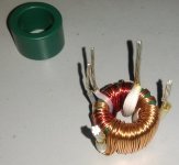
Thanks Dug for your input. for the existing transformer, the secondary winding is winded first.Over that primary winding is done. for the primary, one half is winded one half portion of the core, and other half is winded on the rest half portion of the core. (if you see the transformer pictures you will be clear).
What could be the reason for the regulation? the amp will not have so varying load, only during playing the bass frequency it will draw more current.
I have not putted any load on it yet. I am about to make some high wattage load.
Should the primary RC snubbers be across the transformer coils, rather than across the Fet's?
The secondary RC bits look a bit strange..?
A smallish cap across the secondary will have the biggest effect on the circuit.
Also make sure you have a minimum load at all times if you are not regulating.
I am not sure what is the best idea to place the snubber. I got good results placing them across mosfet rather than transformer. Maybe the experts here may put their opinion which one is more preferable.
The 2ndary R is a little load. C is filtering the high frequency noise if any. There is a TAS5630 amp connected to the 2ndary also.
Ok Forget the secondary, I thought it was some type of buck-boost converter.The MOSFETs are rated as 40V where the max voltage should be (without spike) around 28V. These are for primary. The secondary has 36V, where no MOSFET is present. Is not it enough safety margin ?
Back to a push pull primary.
You will have 2 xVbat on colector/drain , even without spikes, simply because that is the nature of push-pull .
So as you are planning to reach 15V Vbat you are *starting* with 30V peaks ... and that without even the slightest spike, which is to be expected on squarewave or (worse) narrower pulse switchers driving inductive (by definition) loads.
What else did you expect?
And if you are designing for 30V *minimum* (and in practice impossibly low) voltages, then 40V is unsafely close ... hence the 60V up reccomendation.
Your own scope captures prove it.
You might *try* to pad/absorb spikes massively ... which will cause inefficiency and power dissipated uselessly, or you might upgrade to the proper 60V MosFets .
Ok Forget the secondary, I thought it was some type of buck-boost converter.
Back to a push pull primary.
You will have 2 xVbat on colector/drain , even without spikes, simply because that is the nature of push-pull .
So as you are planning to reach 15V Vbat you are *starting* with 30V peaks ... and that without even the slightest spike, which is to be expected on squarewave or (worse) narrower pulse switchers driving inductive (by definition) loads.
What else did you expect?
And if you are designing for 30V *minimum* (and in practice impossibly low) voltages, then 40V is unsafely close ... hence the 60V up reccomendation.
Your own scope captures prove it.
You might *try* to pad/absorb spikes massively ... which will cause inefficiency and power dissipated uselessly, or you might upgrade to the proper 60V MosFets .
Any recommended MOSFET ? the output load is 300W RMS, which gives 30A approx. primary drain current.
Here is the existing transformer causing spike..
If I see well, you wound P1 and P2 on the opposite sides of the core. This is the worst possible method (with highest primary-to-primary leakage). Anything is better. The best is to wind them on the same route.
If I see well, you wound P1 and P2 on the opposite sides of the core. This is the worst possible method (with highest primary-to-primary leakage). Anything is better. The best is to wind them on the same route.
Right you are. they are winded on opposite side. I am planning to rewind them together so that the winding will be like P1-P2-P1-P2-P1-P2... Then after completing will wind the secondary winding. Will share the results after that...
Go to Mouser and search for:Any recommended MOSFET ? the output load is 300W RMS, which gives 30A approx. primary drain current.
Through Hole 60 V MOSFET Through Hole N-Channel 80 A 60 V MOSFET
they have 15 models to pick from.
Starting with 60V 80A TO220 $2.43 3 milliOhms STP140N6F7
What's not to like about it?
Overspec'd on all aspects, which is safe.
http://www.mouser.com/ds/2/389/DM00175190-770678.pdf
That said, try to improve your transformer, never said anything against that. 🙂
- Status
- Not open for further replies.
- Home
- Amplifiers
- Power Supplies
- Inductive Spike for Push-Pull car audio supply