Hello.....
In this circuit, where do the 2 grounds connect to ?
I have the XLR's "pin 1" connected directly to chassis.
The rest of my circuit grounds go to PSU star. That star ground is then connected to chassis through a "loop breaker" (resistor + capacitor).
I'm primarily concerned with the R1-R2 ground.
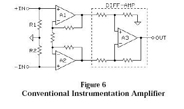
Parts:
OPA2134 (A1, A2)
INA134 (A3)
R1, R2 = 1.5 Meg.
In this circuit, where do the 2 grounds connect to ?
I have the XLR's "pin 1" connected directly to chassis.
The rest of my circuit grounds go to PSU star. That star ground is then connected to chassis through a "loop breaker" (resistor + capacitor).
I'm primarily concerned with the R1-R2 ground.
Parts:
OPA2134 (A1, A2)
INA134 (A3)
R1, R2 = 1.5 Meg.
AndrewT said:Read Rane and Jensen papers.
Andrew, are you tired of seeing these balancing questions here ?
I read the papers, in fact the illustration is from a Jensen white paper.
But of the articles I did read (including Jung/Analog's), I was unable to find any mention regarding where to place those grounds in the schematic, specifically.
It is possible I missed it in the texts, or perhaps it's common sense implementation.....but is not yet common to me....therefore, I asked the question.
Very often I ask a question where I suspect I know the answer, but need confirmation....and I ask it in a way that may be helpful to others who use the "search" function.
Sorry for the mini rant.
I'll connect the R1, R2 ground to "pin 1/chassis" ground, and the other ground to PSU/star ground. I assume R1, R2 are usually placed right at the input XLR pins. I placed them on the board.
R1, R2 are matched.
http://i5.photobucket.com/albums/y177/Midiot/DSCN2946.jpg
=RR=
Sorry,
it wasn't intended to sound like that.
Rane & Jensen, particularly, have addressed this signal grounding issue and why it must be kept separate from the chassis.
it wasn't intended to sound like that.
Rane & Jensen, particularly, have addressed this signal grounding issue and why it must be kept separate from the chassis.

The R1/R2 ground should go to the audio ground.
The XLR pin 1 ground is not part of the audio circuit.
The XLR pin 1 ground is not part of the audio circuit.
R1/2 provide DC bias to the op amp inputs
the balanced signal inputs could be a floating xfmr secondary, or Cap coupled with no DC path
without a DC current path the op amp input bias current would pull the floating balanced inputs beyond the op amp input common mode operating range
The DC path has to return to amplifier power supply/signal ground
jcx said:R1/2 provide DC bias to the op amp inputs
the balanced signal inputs could be a floating xfmr secondary, or Cap coupled with no DC path
without a DC current path the op amp input bias current would pull the floating balanced inputs beyond the op amp input common mode operating range
The DC path has to return to amplifier power supply/signal ground
Yes, correct. The input signal consists of the difference between the two signal inputs, it has no reference to any ground. Of course, it should be *near* ground to stay within the opamps' linear region. The R1,R2 should go to supply ground. Because the output is SE, the output RCA ground pin also connect to supply ground.
Jan Didden
So I have it wrong.....the R1, R2 ground is signal ground, not "pin 1" ground/shield.
Pin 1 goes to chassis, with NOTHING else attached to pin 1.
If I trusted all schematics ( ) , there would have been a "chassis/earth" symbol there , instead of the above signal ground symbol (triangle), if was actually meant to be chassis ground.
Sorry ....I'm but I'm still learning. Thanks for helping me through this. I DO want to learn "why", and not just "how".
I wish it was easy enough to say "Pin 1 to chassis, that's it, forget about it, don't touch it."
...but I see data sheets that components are sometimes (optionally) connected to Pin 1, such as in the THAT 1646 driver datasheet:
Fig. 8
http://www.thatcorp.com/datashts/1600data.pdf
=RR=
Pin 1 goes to chassis, with NOTHING else attached to pin 1.
If I trusted all schematics (
) , there would have been a "chassis/earth" symbol there , instead of the above signal ground symbol (triangle), if was actually meant to be chassis ground. Sorry ....I'm but I'm still learning. Thanks for helping me through this. I DO want to learn "why", and not just "how".
I wish it was easy enough to say "Pin 1 to chassis, that's it, forget about it, don't touch it."
...but I see data sheets that components are sometimes (optionally) connected to Pin 1, such as in the THAT 1646 driver datasheet:
Fig. 8
http://www.thatcorp.com/datashts/1600data.pdf
=RR=
WRT the THAT1600 datasheet, those caps you probably refer to, they are there for RFI/EMI issues. That's why they directly go to the shield (and not actually to pin 1, that is a minor error in the simplifed datasheet drawing). You might want to look at the 1200 line receiver. There you can see that the bias resistors are connected to signal GND (partly internally, via a small "detour"), while these RFI-caps go to shield/chassis. And signal GND and chassis usually have an ohmic conection, not necessarily zero (as drawn). Your mentioned GND breaker, exactly.
The "GND" connection (usually labeled REF with IC's) at the differential amp's output is an input terminal, the reference voltage to which the output of the diff shall be referred to. Should go directly to signal GND, therefore.
A good way to learn is to avoid drawing GND symbols, GND is only a helper construct, a drawing convention with pitfalls (same with supply lines). This sounds funny and might be tedious but really forces one to think about where and what "GND" currents will flow. Better yet, draw each line with an impedance (resistor symbol) to find the points where impedance can be tolerated and where not, changing the net structure (that is, mainly, keep seperate currents seperated, the star point issue. But keep impedance and loop area low, that's why usually a continuous GND plane is the preferred solution, depending on currents and frequencies involved).
- Klaus
I bow to your superior knowledge gentlemen. All I'll say in my defense is that I have built probably half a dozen implementations of that circuit and never had any issues with connecting the input ground to pin 1. 😉
I just got here, but pin 1 only is really dangerous, even if it may be logical. In my designs, I usually don't DC couple the power supply ground to the chassis. Big problem when only pin 1 is used for DC biasing the input.
Al,
no problem with that, I did that myself often without any problem, and had to connect XLR1 to signal GND anyway because combo inputs were used (XLR/TRS combo receptacle). It only offers more potential for problems when you have a lot of RF around and/or have peaks of maybe several amps of shield current (if you ie connect from building to building, spanning 300ft or so).
@John:
I'm not sure if I understand your comment...
- Klaus
- Status
- Not open for further replies.
- Home
- Amplifiers
- Solid State
- INA134 unbalancing....quick question...