Re: i like your design very much,and ...
This output stage is a follower, so the gain is near 1 and the output impedance is low.
Cheers
Alex
john-china said:how much is the gain. and how to caculate it?
This output stage is a follower, so the gain is near 1 and the output impedance is low.
Cheers
Alex
it is amazing
the whole picture which you post above is a follower, isn't it. just like
common drain circuit (emmiter follower) .
so if i want to build a amplifier with this circuit, i must add input and VAS circuit. is what i think correct?
and another question. i only have irfp240 , so how should i do this circuit beacause of zvp3310 bias problem. i can not connect gate of zvp3310 to output directly. give me detailed resolution, pls.
Re: it is amazing
Yes, that is correct.
You can not use this particular circuit with irfp240 - only Logic Level N-ch MOSFETs will work (i.e. IRL540 or 2SK1530 etc.). For IRFP240 you would need to change the arrangement to include an additional bias for P-ch device. I did not try it so I can not offer you a ready circuit for that. It should be possible, thought. One more thing about using IRFP240 - you'll lose much more voltage out of the supply rails , the current source would need a boosted (by 5-10V) separate supply and the temperature compensation needs to be be different.
Overall - it is not easy to replace the o/p devices here for "non LL", sorry. Look for IRL540 - they are quite common and cheap - and good for up to about 50W output per pair.
Cheers
Alex
john-china said:the whole picture which you post above is a follower, isn't it. just like
common drain circuit (emmiter follower) .
so if i want to build a amplifier with this circuit, i must add input and VAS circuit. is what i think correct?
Yes, that is correct.
john-china said:and another question. i only have irfp240 , so how should i do this circuit beacause of zvp3310 bias problem. i can not connect gate of zvp3310 to output directly. give me detailed resolution, pls.
You can not use this particular circuit with irfp240 - only Logic Level N-ch MOSFETs will work (i.e. IRL540 or 2SK1530 etc.). For IRFP240 you would need to change the arrangement to include an additional bias for P-ch device. I did not try it so I can not offer you a ready circuit for that. It should be possible, thought. One more thing about using IRFP240 - you'll lose much more voltage out of the supply rails , the current source would need a boosted (by 5-10V) separate supply and the temperature compensation needs to be be different.
Overall - it is not easy to replace the o/p devices here for "non LL", sorry. Look for IRL540 - they are quite common and cheap - and good for up to about 50W output per pair.
Cheers
Alex
Re: Re: it is amazing

x-pro said:
You can not use this particular circuit with IRFP240 - only Logic Level N-ch MOSFETs will work (i.e. IRL540 or 2SK1530 etc.).
Cheers
Alex
Re: A Nice Tweak from N-Channeler
Yes, that is exactly what I've described in my previous message in this thread 🙂
Cheers
Alex
Workhorse said:To use that circuit with Standard Gate drive Vertical N-channel Mosfets/Igbts
Here is an enhancement[a nice tweak]🙂
which will also offer rail to rail performance as an added bonus!!
Yes, that is exactly what I've described in my previous message in this thread 🙂
Cheers
Alex
Thank you for nice article.
I read your article with PLH again.
some months ago my question about PLH was contribution of upper/lower driver and biasing. And ask NP about that.
After reading your article ,I understood some biasing issue.
I read your article with PLH again.
some months ago my question about PLH was contribution of upper/lower driver and biasing. And ask NP about that.
After reading your article ,I understood some biasing issue.
The most linear output N channels at this point are the Silicon
Carbide JFETs out of SemiSouth. They have a fraction of the distortion
but are very expensive and difficult to get.
😎
Carbide JFETs out of SemiSouth. They have a fraction of the distortion
but are very expensive and difficult to get.
😎
Nelson,
would you mind to share some bread crumbs why this is the case (that is, as far as you have determined the root causes)?
Has it to do with a closer to ideal quadratic transfer function in general, or is it a distortion cancelling "load line trick" that works better with them?
- Klaus
would you mind to share some bread crumbs why this is the case (that is, as far as you have determined the root causes)?
Has it to do with a closer to ideal quadratic transfer function in general, or is it a distortion cancelling "load line trick" that works better with them?
- Klaus
However, privileged electrical conditions are needed for any device to exhibit the lowest possible modulations of their parameters, but in case of SiC the main advantage is in the material itself that on the same working temperatures is much better than other known semiconductors. SiC BJTs are also very promising. You can't eliminate current modulation effects when the load is complex, but they can be minimized by topology and better devices used.
Wow!
Nelson, these seem to have around 15-20S in the 'aleph friendly' region of operation, compared to probably around 2-3S of IRFP240 !
Now, that would be some considerable upgrade!!
Nelson, these seem to have around 15-20S in the 'aleph friendly' region of operation, compared to probably around 2-3S of IRFP240 !
Now, that would be some considerable upgrade!!
Because they are so unique, and I think might appeal to many here, I have started a new thread to discuss the SiC JFETs in here:
SemiSouth Power SiC JFETs
SemiSouth Power SiC JFETs
RocketScientist said:Because they are so unique, and I think might appeal to many here, I have started a new thread to discuss the SiC JFETs in here:
SemiSouth Power SiC JFETs
Thank you. They were discussed the first time in Syn08's thread, when we mentioned Kirk and Early effects in transistors.
http://www.diyaudio.com/forums/showthread.php?postid=1835074#post1835074
in this case also the follow thread could be of interest:
"Only N-Channel MOSFETs (NMOS); better Audio from non complements by Audio Power?" - go to
http://www.diyaudio.com/forums/showthread.php?s=&postid=1898865#post1898865
"Only N-Channel MOSFETs (NMOS); better Audio from non complements by Audio Power?" - go to
http://www.diyaudio.com/forums/showthread.php?s=&postid=1898865#post1898865
Could anybody point out possible advantages/disadvantages of Nikitin's output buffer stage compared to Andrea Ciuffoli Power Follower, except for their different class ( A/B and A) ? Maybe somebody listened both?
Last edited:
Alex,
accomplishing several things in one blow sometimes mean compromising. The task of a phase splitting stage is to generate two balanced differential signals, most importantly, being accurately 180° out of phase and equal in amplitude. The gate-source and gate-drain properties are not equal. To noticeably linearize the output devices, the CFP could be a way to go.
Klaus,
that`s a nice circuit in post #18, when M5/M6 JFET, M3/M4 bipolar.
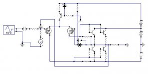
I am happy to invite forum members to have a look at my short article:
http://www.ant-audio.co.uk/Theory/N-channel D-MOSFET output stage with improved linearity.pdf
In this thread I will try to answer questions about that circuit configuration and also about the last diagram from the article - a practical example of an output stage that can be used with or without an overall NFB with either tube or solid-state VAS. I attach this circuit diagram here as well.
Alex Nikitin
I have found this URL about an additional distortion removal circuit
Distortion removal circuit
Here the automatic translation in English
Google Übersetzer
what do you think about this topology?
I am happy to invite forum members to have a look at my short article:
http://www.ant-audio.co.uk/Theory/N-channel D-MOSFET output stage with improved linearity.pdf
In this thread I will try to answer questions about that circuit configuration and also about the last diagram from the article - a practical example of an output stage that can be used with or without an overall NFB with either tube or solid-state VAS. I attach this circuit diagram here as well.
Alex Nikitin
Which commercial brands (except Creek) uses this topology?
- Home
- Amplifiers
- Solid State
- Improving the linearity of an N-ch MOSFET output stage