Hi,
I made this kind of experiences using real components and a little 10 Mhz scope 25 years ago .
A must is having V2 stable. Jung considers it as bootstrapped to the negative power supply rail.
I obtained excellent results from circuits like those built around Q1 or Q10, picture post #38.
Even without decoupling V2, impressive results came from an NFB circuit using a TL431 in place of Q2. As far as I remember, it was not temperature sensitive but probably noisier and less stable with transients at the collector of Q1 than the circuits of the picture.
Walt Jung's papers :
http://www.audioxpress.com/magsdirx/ax/addenda/media/jung2778.pdf
http://www.audioxpress.com/magsdirx/ax/addenda/media/jung2779.pdf
It was completed in readers mail in a following issue.
Last edited:
A PNP version would be the mirror image of the N version. But in general, the PNP member of a complementary pair is slower and has larger capacitances than its N counterpart, which means the ringing will be stronger and lower in frequency.Elvee,
Can you please simulate a PNP-version of your CCS improved with resistor (and if possible the improved cascoded CCS).
Would the result be comparable to the NPN-version, or would there be any difference?
But you are free to choose low-capacitance transistors, fe. a BF450 for the sense transistor, and a high performance video output transistor for the regulator.
It is one of the options to remove the ringing. Another one, which has less impact on the dynamic performance is to put the capacitor between V- and the base of the output transistor. Also, the 1n value is a bit high, 100p would be sufficient.Interesting results so far.
I have another thing to throw in: A small cap between the bases of the feedback version. What do you think about this idea? (it wasn't mine but I used it in an amp) I don't like the overshoot somehow and the rounded corner looks more friendly to me... Is this any good?
This thread was initially created to show that the regular, non-decoupled circuit is sensitive to V2, and that by adding a single resistor, this sensitivity could be reduced by an order of magnitude.Hi,
I made this kind of experiences using real components and a little 10 Mhz scope 25 years ago .
A must is having V2 stable. Jung considers it as bootstrapped to the negative power supply rail.
I obtained excellent results from circuits like those built around Q1 or Q10, picture post #38.
Even without decoupling V2, impressive results came from an NFB circuit using a TL431 in place of Q2. As far as I remember, it was not temperature sensitive but probably noisier and less stable with transients at the collector of Q1 than the circuits of the picture.
Walt Jung's papers :
http://www.audioxpress.com/magsdirx/ax/addenda/media/jung2778.pdf
http://www.audioxpress.com/magsdirx/ax/addenda/media/jung2779.pdf
It was completed in readers mail in a following issue.
Using a TL431 would indeed greatly improve the low frequency performance, and practically eliminate the temperature dependence.
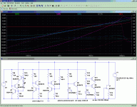
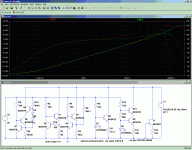
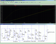
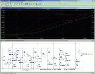
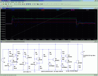
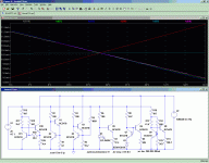
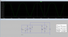
Now, here is the behavior in the frequency domain.
We recognize the elements seen in the time domain, in particular the strong ringing just slightly above 100MHz for Q8.
The responses of Q1 and Q3 are identical.
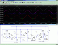
If a base stopper is added to Q2, the effect is to create a bump in the response under 100MHz.
The following pic shows the effect of a neutralizing capacitor: C2 clearly gives the best result, leaving the frequency response an ideal slope, caused only by the collector capacitance.
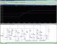
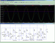
If a low-capacitance, HF transistor is substituted for Q3, the HF performance is improved, and becomes better than the jFET (the BF245 is also a VHF transistor).
The low-frequency behavior is somewhat degraded, due to the lower gain of the BF240.
Attachments
Here it is, but don't jump to conclusions.
Hi,
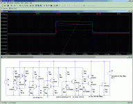
as I suspected, the feedback CCS has ripple and more variation when pulsed signal is applied.
I did not jump to any conclusions.Elvee,
can you do a stability sim for these three versions?
I suspect the two feedback versions will be quite different from the LED version.
I first asked for stability comparisons and proposed that the feedback topology would be quite different from the LED version.
I then saw your report and could see evidence that the stability was different between the two topologies.
Now your simulation report shows a very distinct difference to step response.
I like what I see for IcQ5 and IcQ10.
The excessive overshoot and ripple in the feedback versions does not seem desirable for good audio quality.
A final request,
compare the LED versions to the compensated feedback versions for step response to both voltage supplies.
Last edited:
Here it is.A final request,
compare the LED versions to the compensated feedback versions for step response to both voltage supplies.
But once again, be careful at interpreting what you see: with the simulator, we are able to zoom in on a tiny portion of the signal, both in time and in amplitude: it is an event of 100ns X 250µA for most versions, except the jFET.
In terms of signal energy, the disturbances caused by the circuits you prefer are in fact higher.
They might be more pleasing to your eyes but remember, you don't hear with your eyes.
Ringing and other artifacts are not audible by themselves: their spectrum sits at 100MHz and above. They could have an impact if they upset the bias levels, or cause any other form of intermodulation, which is not the case here, even though the conditions are pretty extreme, with a 100ns step having a non-limited spectrum.
Note that I am myself an adept of extreme tests: if you shake something violently enough, you can get valuable information from the misbehavior's, failure modes, etc. But you have to remain reasonable in the interpretation.
Finally, here is a test where all the versions have bypass capacitors of minimal, but sensible values:
Attachments
Elvee,
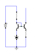
Give a try to Zener based CCS.
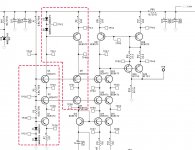
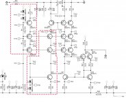
Here it is, plus one or two more variants:
With Q9 and Q8, the zener is emulated by a Vbe multiplier, but with a twist: R12 provides a compensation for the dynamic resistance of the reference element.
Q11 and Q10 is an hybrid between this circuit and the regular two transistor CCS.
The performance of the three compensated circuits is markedly superior to that of the others, even the zener-referenced one, which requires a substantial voltage to operate.
Attachments
The performance of the three compensated circuits is markedly superior to that of the others, even the zener-referenced one, which requires a substantial voltage to operate.
Thanxz for the effort,
Thats why i always use Zener referenced CCS, I usually use a 3.6V 500mW zener with Iz=5mA and sometimes a 15V 1W Zener with Iz= 10mA for dedicated high voltage based CCS.
Also with a substantial voltage across CCS due to Vz, the noise injection is somewhat less from the rails.
Kanwar
It is the functional equivalent of a lambda diode, but capable of operating at much higher levels.
The most recent issue of QEX had an article "Playing with the Lambda Diode" -- here are a couple examples they cited with the DC analysis:
An externally hosted image should be here but it was not working when we last tested it.
An externally hosted image should be here but it was not working when we last tested it.
The 2N4124 is supposed to use a 2n2219 transistor which I haven't simmed. I guess it must be a high speed switching transistor.
Simply miswire your 2n2222 with emitter toward plus, collector toward minus, base open.
Don't need any of those other parts... Can't sim a miswired 2n2222 negistor, or can you?
Breaks over about 9V...
I thought Lamda Diode was a pair of JFETs?
Anyways, can't think any use for negistor in a current source or sink?
The point seemed to be, that compensation should never bend your
loadline down so much that any part of it becomes a negative slope.
You just want it flat, not more than flat....
Then Elvee will prove me wrong with some Xquad based current source.
Last edited:
I thought Lamda Diode was a pair of JFETs?
See the article -- lots of device combo's to derive the same I-V effect.
I searched first and found this thread to be one which discussed Lambda diodes, kinda tangential to the topic at hand...
That is true, but the effect is not predictable: some parts will simply behave like a zener, with practically no negative resistance effect.Simply miswire your 2n2222 with emitter toward plus, collector toward minus, base open.
Don't need any of those other parts... Can't sim a miswired 2n2222 negistor, or can you?
Breaks over about 9V...
The effect is caused by the gain droop at low current: the Vceo to Vcb ratio depends on a power of beta, and if the beta remains constant, there is no change and therefore no negative resistance.
Older transistor processes yielded relatively poor quality devices and the effect was very pronounced.
Modern transistors are of better quality and do not show the effect.
It can be simulated/enhanced by connecting a large value resistance between the base and emitter (or base and collector, if it is used in reverse).
The original lambda diode was a pair of complementary FETs, symmetrically connected, but the term has been extended to anything two wire/two transistors having a negative resistance.I thought Lamda Diode was a pair of JFETs?
This is the closest bipolar equivalent of a true lambda:
Not this time, but I have proposed a very incestuous type of CCS:Anyways, can't think any use for negistor in a current source or sink?
The point seemed to be, that compensation should never bend your
loadline down so much that any part of it becomes a negative slope.
You just want it flat, not more than flat....
Then Elvee will prove me wrong with some Xquad based current source.
http://www.diyaudio.com/forums/solid-state/197104-improved-2w-current-sources-ii.html
Attachments
Hi Elvee
I am searching to improve the VAS CCS on my power amp that uses a typical two BJT thing.
Walt Jung clearly states that this topology should be avoided due to possible instabilities so I would like to use a LED reference instead.
Your modification produces outstanding results in sim so I transported it to the LED ref also.
In my simulation the CCS rejection is even higher but I do not know if it does work in reality.
Would you please comment on my schematic ?
Best
Ricardo
Attachments
It will work in reality, but with a few caveats: the rejection will be optimal for a single value of V2 only.In my simulation the CCS rejection is even higher but I do not know if it does work in reality.
The circuit relies on a bridge of 4 resistances: R8 Rd(D1) and R11 R7.
When the bridge is balanced, the Vbe of Q6 remains unchaged against V2's variations, meaning its collector current is also unchanged.
For large variations of V2, two effects will perturb the cancellation: D1's dynamic resistance will change, and the currents in R8 and R11 have different slopes and offsets wrt.V2, because there is one Vbe difference.
For low voltages and large variations, this will ruin the cancellation, but in a normal amplifier circuit, this shouldn't be an issue
The dynamic resistance of the diode obeys the same law as for other junctions:
Rd=26/Id, with Id in mA and Rd in ohm, but a non-Si diode may have unusual non-ideality parameters, ohmic contacts, etc., which means an actual test is probably your best option: build the CCS, feed it with a rippled supply and select R11 to get the optimum rejection.
Note that this will be valid only for the type of LED you used for the test: even an identical-looking but different LED could have completely different parameters.
Also remember that any attempt to bypass the LED with a capacitor will completely destroy the compensation at high frequencies.
HelloI don't mind adding a resistor, but I don't like the idea of adding one more lytic to anything.
And a shunt regulator might be a bit of an overkill.
On the other hand, adding this resistor costs practically nothing and does bring a substantial improvement, both dynamically and statically.
OK, let us do it properly: the formula I guessed in the first post was incorrect (I am becoming lazy with age).
If we look at CCS1, we see that the output current is determined by RE and the Vbe of Q2.
This Vbe is in turn dependent on the bias current, provided by VB and RB.
Because there is a logarithmic relationship between IB and Vbe, this means that this circuit is in fact a (crude) logarithmic converter: Iout is the logarithm of VB.
CCS2 shows the situation with the compensating resistor RC. The dynamic emitter resistance of Q2 is shown explicitly, and we can see that for the compensation to occur, the division ratio of RB to re has to be identical to that of RC to RE: this gives the relationship indicated on the schematic.
This is a first order simplified analysis, valid on the conditions variations are small, and bias current is sufficiently high, etc, but it shows the compensation is essentially device-independent.
With the values of the previous example, the formula yields a result of 43K, which is not too far off the mark.
Obviously, the compensation cannot be perfect: a linear compensation will never cancel a logarithmic effect, but for practical purposes, it is useful enough as the example shows.
1. How to calculate RE (resistor emitter Q1) based on given equation?
2. What is the function of re (resistor on emitter Q2)? Why only mention one time? Is it important?
Thank you
Last edited:
RE is calculated the usual way for a CCS: RE=Vbe/I. The actual value will need to be slightly smaller due to the correction resistor, but it is a good starting point.
The schematic you posted is just explanatory, and the implicit emitter resistor re (part of the transistor) is explicitly shown for more clarity. You do not need to implement it physically.
The schematic you posted is just explanatory, and the implicit emitter resistor re (part of the transistor) is explicitly shown for more clarity. You do not need to implement it physically.
- Home
- Amplifiers
- Solid State
- Improved current source/sink