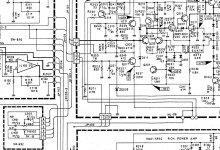
Ugh. I found another difference between the Nad 2600A (the unit in front of me) and the 2700 schematic. And it's a big one!
In the "power envelope" rail-lifter circuits, the schematic shows 24V zeners at ZD305 - ZD308. This starts to lift the supply rail when the output rail comes to within 24V of it. The unit in front of me has 6.8V zeners instead.
The 24V zener lifts the supply fairly early, maybe unnecessarily so? It produces more "false alarm" supply-rail lifts when the program material would never clip at the lower rail.
I'd love to know why the factory made this change. The 6.8V zener allows outputs' collector voltage to get quite low before the "boost" so maybe they get into a region where hFE is low and collector capacitance is high. Maybe it's a stability thing. But going to a 24V zener seems a bit much -- if the 6.8V was marginal, you'd think a 10 or 12V part would give enough headroom.
I blueprinted the rest of the rail lifter subcircuit, and the 2600A matches the 2700 schematic for everything else. Only the zener value changed.
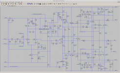
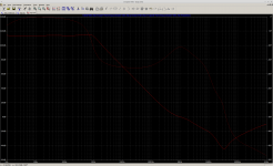
One more change! Now it's really final :-D
As in comment 6, this change concerns solving the ~1kHz peak in loopgain that can result from TPC.
I deleted the series R1=390k and C1=39p across the VAS transistor. It turns out that this arrangement depends on the beta of the VAS buffer, and we don't want to depend closely on any transistor's beta. Whoops.
That's OK because here's an even better arrangement. It loads the VAS less, it adds minimal load to the IPS (maybe less than before) and it's very easy to shape the loopgain plot and choose how much you'd like to reduce the 1kHz peak.
The new R/C pair at the IPS tail reduces loopgain a little bit, so I shrunk the IPS emitter degeneration resistors to cancel that.
This sounds better! (I think!) It sounded a bit nasal before, like there was some treble exaggeration. That's gone. I was surprised that this change was audible. Why was it audible?
The new R-C network reduces differential-mode impedance at the IPS tails, especially at treble frequencies. That could make the IPS less prone to pick up stray EMI from halfwave-rectified output currents. That's a guess. (The layout doesn't do as much as you'd like to isolate the IPS from halfwave rectified currents.) I can't quantify the benefit, but it can't hurt to lower IPS impedance at treble and above.
Final (haha) schematic and loopgain plots below.
Attachments
The smooth warm powerful tone this amp has - what happens to that, with this mod?
On my L65 Jubal I could use more mid tone focus/punch and slightly tighter bass.
On my L65 Jubal I could use more mid tone focus/punch and slightly tighter bass.
Oooh, there's an error in the grounding architecture on this 2600A.
The ideal ground star is actually a "vine", with the largest and least signal-like currents at one end and only tiny, signal-like currents down at the other end where the ground is used as a signal reference. No trace has zero impedance, currents always induce voltage drops, so there is no single "ground." But we can arrange the vine so the worst errors are separated from uses of ground as a signal reference voltage. This is a good ground vine:
+---> transformer center tap
|
A // Leg A carries huge, non-signal-like currents
|
+---> filter cap grounds
|
B // Leg B carries large signal-like currents from the speaker returns
|
+---> speaker return grounds, output stage zobel return
|
C // Leg C carries small, mostly signal-like currents
|
+---> chassis, general small current ground points
|
D // Leg D carries near zero current. You can add a 5.6 ohm resistor
| // at D to further isolate the signal-reference line from the chassis ground.
|
+---> signal reference for power amp input network, unbalanced input shields
That's not what we have on the 2600A, from the factory it looks like this:
+---> filter caps
|
+---> output stage zobel return
|
+---> chassis and speaker return grounds. (Elsewhere on the chassis it
| connects to the small signal grounds and signal reference line.)
|
+---> transformer center tap
This is not great. The whole spine of this vine carries charging spike currents. Let's arbitrarily consider the chassis to be the best, true, 0V ground (so that everything hanging off the chassis is also 0V.) This arrangement can still couple charging spikes into the output stage through the zobel return. Also, the power rails will bounce along with the charging spikes, moreso than in the ideal arrangement.
It's an easy fix: cut one trace and solder in one short (and heavy) wire to bring the transformer center tap in right where the filter caps meet. That transforms the ground vine to be nearly ideal.
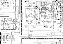
While doing some work on my 2600a I discovered there is no 2600a manual that I could find so was using the 2600 but there are some differences. The 2600a is a cross between the 2600 & 2700. Using only the L channel in these examples, C215, 217 are not there in the 2700 or 2600a. C310, 303 in the 2600 are 4.7/100 and in the 2700 & 2600a, 100/100. My 2600a has these glued to the solder side of the pcb. For better filtering I can see.
But especially C207 in the 2600 & 2600a 220/10 vs 680/63 in the 2700. And C901, 902 - 10/25 in the 2600 & 2600a and 47/25 in the 2700. C203, 204 - 10/25 in the 2600 & 2600a and 47/25 in the 2700....what effect on sound would they have? Would it be a good thing to change these in a 2600a to match the 2700?
But especially C207 in the 2600 & 2600a 220/10 vs 680/63 in the 2700. And C901, 902 - 10/25 in the 2600 & 2600a and 47/25 in the 2700. C203, 204 - 10/25 in the 2600 & 2600a and 47/25 in the 2700....what effect on sound would they have? Would it be a good thing to change these in a 2600a to match the 2700?