Seasons Greetings all.
A quick and possibly the last 'stupid' question of 2010.
I was thinking of producing a couple of JE990 discrete opamp PCBs. The files I have found on the web. Looking at the layout I see the components are pretty much all over the place. Is there a design/ layout rule one MUST follow or is it a case of trying to fit everything in to a small space.
I ask this because I just opened a friends integrated amp and have seen the preamp stage is basically a discrete opamp design but takes up about 90mm x 90mm. The layout was as if copied from a schematic layout.
The JE990 pcbs posted on the web as well as the modules you can buy take up about 30mm x 30mm but the layouts are VERY different to the schematic layout.
If I copied the layout from the schematic (as in the schematic) and made my own which took up a space of say 30mm x 30mm would there be any problems - noise, distortion etc.
Thank you
Rob
Hi Rob - Take a look at this PCB Printed Circuit Boards Design and Layout
There are a lot of sites that give pointers - but good PWB design and layout is a bit of a learned "art" just as is good circuit design. Have a go at it - it's the best way to learn.
There are a lot of sites that give pointers - but good PWB design and layout is a bit of a learned "art" just as is good circuit design. Have a go at it - it's the best way to learn.
What excellent reading. One of the best things I have read all year.
According to what I have read and other bits, high voltage and high frequency layouts need MUCH more care than low frequency low voltage (audio) - is that correct?
I'm going to give a layout a go and get it produced as these things now only cost a few $ but more in time.
Thanks for the site.
According to what I have read and other bits, high voltage and high frequency layouts need MUCH more care than low frequency low voltage (audio) - is that correct?
I'm going to give a layout a go and get it produced as these things now only cost a few $ but more in time.
Thanks for the site.
What excellent reading. One of the best things I have read all year.
According to what I have read and other bits, high voltage and high frequency layouts need MUCH more care than low frequency low voltage (audio) - is that correct?
I'm going to give a layout a go and get it produced as these things now only cost a few $ but more in time.
Thanks for the site.
Yes - HV and HF circuits require care in their design and layout - but you can learn some nice tricks and methods by learning from their examples.
If you get into playing around with DAC's or clock circuits - well things can get away from you quickly if sound design practices are not followed. Many analog amps are capable of response into several megacycles and thus problems with interference as oscillations can occur - and this can be minimized with good design. Signal paths, effective grounding, and power supply reserve - these are key aspects to look at when designing these little toys. There is a lot to learn - don't let that get you down - when (or if) you get stuck or need to ask a question there are a lot of very talented people here that will be glad to help you out. 😀😀😀
Yes, in many cases digital circuits, even quite high speed ones, will work quite happily with haphazard layouts, but analog circuits can be more sensitive. With digital there may be EMC (radiated or conducted) problems.
It's true that RF circuits are generally more problematic than AF, sometimes requiring a complete Faraday cage (metal box) and feedthrough caps for some sections, but layout, particularly grounding, can still have a big impact at AF, affecting noise performance, and, if inputs are close to outputs, there is the possibility of feedback.
w
Hi R - here is a bit of reading for you - http://www.pcb123.com/tutorials/PDF Documents/PCBDesignTutorialRevA.pdf
http://pcbwizards.com/education.htm
😀
http://pcbwizards.com/education.htm
😀
Seasons Greetings all.
A quick and possibly the last 'stupid' question of 2010.
I was thinking of producing a couple of JE990 discrete opamp PCBs. The files I have found on the web. Looking at the layout I see the components are pretty much all over the place. Is there a design/ layout rule one MUST follow or is it a case of trying to fit everything in to a small space.
I ask this because I just opened a friends integrated amp and have seen the preamp stage is basically a discrete opamp design but takes up about 90mm x 90mm. The layout was as if copied from a schematic layout.
The JE990 pcbs posted on the web as well as the modules you can buy take up about 30mm x 30mm but the layouts are VERY different to the schematic layout.
If I copied the layout from the schematic (as in the schematic) and made my own which took up a space of say 30mm x 30mm would there be any problems - noise, distortion etc.
Thank you
Rob
Short paths , special attention to grounding , and most important ... the thermal aspect. By this I mean "face to face" differentials (original je-990 )
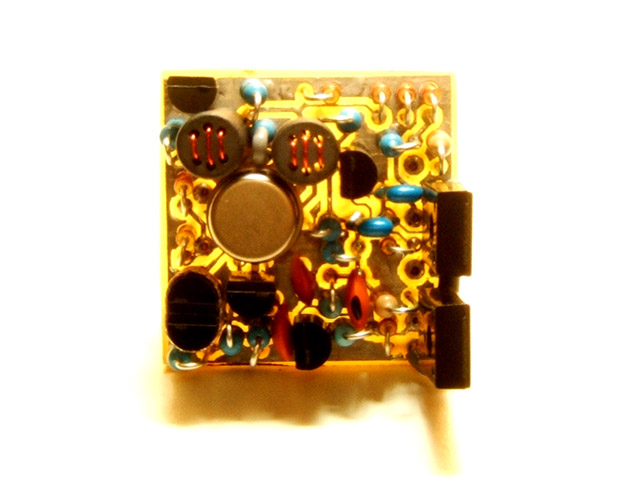
, every section that has gain thermally coupled (like the JE or mine - attachment). With this "style" , my module can be put outside in the cold (-10C), turned on and heated to 60C with a hairdryer ... staying within .5mv offset over the whole range. If you want precision , layout is a major issue. Keep similar functions grouped together as "blocks" on the PCB (IPS ,VAS , CCS). Good luck !
Wow , the je-990 is the "baby" to my module .. same dang thing , just little with no CCS.
OS
Attachments
Last edited:
I don't know if this makes me a "thread necromancer", but I stumbled on this thread and wondered . . . "How is the project going?".I was thinking of producing a couple of JE990 discrete opamp PCBs. . . .
As a contribution to the discussion, I think many of those PWB layouts for the '990 are trying to duplicate the mechanical footprint and pinout of some potted, discrete amplifier modules from the 1960's and 70's.
I am convinced that PWB layout is an art that you master by practice. I also firmly believe that a good PWB layout guy (or gal - one of the best I've worked with is a female girl person of the opposite sex) is often the most under-appreciated member of a product design team. The web links posted here (and many others) give excellent guidelines but they aren't a cookbook - any more than memorizing a grammar book and a style manual will put you in the same league as Hemingway or Dickens.
In general terms, forcing a large number of components into a small physical volume increases the electrical, thermal, and vibrational coupling of the circuit. Sometimes this is desirable - as in maintaining a common temperature for the input differential, or output driver, pairs; or minimizing the current loop and unclamped inductance of an SMPS. In other cases it's problematical, as when a thermal "wave", propagating from a sudden increase in output loading, upsets the biasing of other stages.
If you post Gerber files, or even a screenshot of your layout, you can probably collect at least a few useful comments.
Dale
- Status
- Not open for further replies.
- Home
- Amplifiers
- Solid State
- Importance of layout