SOA
The SOA, as mentioned above, is the safe operating area for the device. If you look at the SOA graph, you will see a line that connects all allowed currents and voltage combinations. You would expect a straight line. For instance, for a 100W device, that would mean 10 amps @ 10 v, 5 amps @ 20 V etc. However, you can NOT run 1 amp @ 100 v, because a phenomenon called secondary breakdown will destroy the device. Well, yes you can run 1 amp @ 100 v but not as DC, only for limited period. Again, see the SOA curve.
Where this comes into play is in audio amps that drive a reactive speaker (and all speakers are rective at some point in the freq range). In those cases, output voltage and output current in the speaker are not in phase. That means that you can have an output voltage close to the pos rail, while the current goes to the neg rail. For the bottom transistor that means almost the full rail-to-rail voltage at a relatively high current. You are then in a SOA part that can be sustained for only a short time.
One remedy is to add several output devices in parallel or use devices with a much higher Vce than required for the rail voltages.
This is the reason that you often see an output stage power capacity seemingly much higher than would be required for a 8 or 4 ohm resistive load.
Jan Didden
I know nothing about IGBT's than what ive just read here.
But from what i have just read, Class-D application comes to mind.
Would they suit this as a cheaper alternative to MOSFETs?
But from what i have just read, Class-D application comes to mind.
Would they suit this as a cheaper alternative to MOSFETs?
Hi,
what do you want to know about the IGBT-amplifiers?
I've built 2 HEXFET versions (IRF540/IRF9540), 5 IGBT versions (GT20D101 and GT20D201) and 2 IGBT-subamps (2 pairs of GT20D101 and GT20D201)....
Grtz, Joris
what do you want to know about the IGBT-amplifiers?
I've built 2 HEXFET versions (IRF540/IRF9540), 5 IGBT versions (GT20D101 and GT20D201) and 2 IGBT-subamps (2 pairs of GT20D101 and GT20D201)....
Grtz, Joris
i basically want the most cost effective way of getting 200w for a sub.... since igbt seamed cheap compared to mosfets... i thought of using igbts.....
Since this is all you want, I say go ahead. Build the channels
balanced (or bridged) using only two devices on each half
(4 total) per channel.
Since matching and SOA are a pain with IGBT's, this approach
will circumvent these problems. No parallel devices, and
low voltages.

balanced (or bridged) using only two devices on each half
(4 total) per channel.
Since matching and SOA are a pain with IGBT's, this approach
will circumvent these problems. No parallel devices, and
low voltages.
If you wanted to use only N-channel IGBT's (therefore giving you a much wider choice of devices) maybe you could adapt the cct of Anthony Holton's N-channel amplifier.
Better set Infineon straight then.
Well, looky here...djk said:
There is not one piece of data published on the forward biased safe area of these large IGBTs.That is because they are not designed for linear use. The SOA is just like that of a BJT switching transistor, NONEXISTENT !!!
How nonexistent is nonexistent?
Attachments
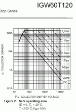
That's an interesting curve insofar as it exhibits no
second breakdown for the bipolar component of the
transistor, all the way to 1000v.

second breakdown for the bipolar component of the
transistor, all the way to 1000v.
Is your left leg shorter than your right?hacknet said:as linear as the line dividing my ****... how much does it cost?
hacknet said:as linear as the line dividing my ****... how much does it cost?
Did you notice it is a log-log graph? Try plotting the same on a linear x-y graph sheet!
on this igbt thing, it seems to be picking up the worst of both worlds: thermal breakdown of bjt and gate capacitance of mosfet.
Has anyone tried to make the reverse of igbt? that is, a bjt pre-drive and mosfet power stage on one die? it will have low input capacitance of a bjt and thermal characteristics of a mosfet. the die temperature is still a problem tho.
Has anyone tried to make the reverse of igbt? that is, a bjt pre-drive and mosfet power stage on one die? it will have low input capacitance of a bjt and thermal characteristics of a mosfet. the die temperature is still a problem tho.
- Status
- Not open for further replies.
- Home
- Amplifiers
- Solid State
- IGBTs