fast slopes
Please ignore the shaded region of the image, that circuit does not apply.
A suggestion for faster switching in a half-bridge UcD. The idea is that once the drain starts falling in respect to the source, the opposed body diode has already stopped conducting, and nothing will take damage if you switch a little faster than during discharge of Qrr (as long as you stay below the dv/dt capability of the mosfet).
Am I correct that this circuit should lessen the problem with the miller capacitance causing flat spots in the Vgs curve during switching?
If you let Vgs of the output devices cross at Vth high enough to never allow any current to freewheel into the body diodes (higher than any peak current entering the output filter), this circuit should be possible to use with very little dead time?
hi zilog,
nice idea...
but: if output coil current switches - at low modulation - you have 20ns (about) switching anyway,
and at high current, output will switch only, if opposite fet draws >> current, so no speed-up here...
nice idea...
but: if output coil current switches - at low modulation - you have 20ns (about) switching anyway,
and at high current, output will switch only, if opposite fet draws >> current, so no speed-up here...
kartino said:let see your simulation.... just see as short way to know
Yes simulate it if you really want a picture of what's going on. When you want things to happen fast within a few ns, you have to simulate it due to the complexity of all the nonlinearities and parasitic capacities in the transistors.
I do think that you'r configuration will give you faster slopes, but what you really want is to turn the upper FET OFF fast and the lower one ON just afterwards, or vice versa. My experience with the UCD comparator and gate driver combo solution is that the comparator part of it is to slow as well as the gate driver. If the comparator was faster and had more gain it would supply square shaped currents to the gate driver, which would help a lot. Also the fact that the actual gate driver circuit uses a pull-down resistor to turn the respective gate off, really gives you a long turn off time due to the lumped capacities in the driver
transistors.
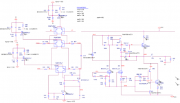
I've attached a whole new comparator + gate driver configuration below. The comparator has a propagation time in the region of 50-80ns and the gate driver is much faster than the UCD solution. Especially the active differential level shifting to the upper gate driver works fast. The downside is that the of the upper and the lower gate driver circuits are not the same, which can make matching difficult. I do think however that it would be possible to copy the upper gate driver circuit and use it for the lower part.
If you want to stick to the UCD solution, then add active differential level shifting instead of using pull down resistors. This really improves the turn off steed of the FETs, which gives the possibility to work with a smaller deadtime.
Attachments
This my arrangement looked good as Kaspar said for more gain for gate current. But I have no time to try at real. In my experience there will be problem in cross conduction at real.
Don't look the complexity, we can even make simpler. I have posted similar before, but this is new changing.
But we still waiting for what cooked by Zilog now.
Don't look the complexity, we can even make simpler. I have posted similar before, but this is new changing.
But we still waiting for what cooked by Zilog now.
Attachments
I can see that you've added a gain stage, which is one
improvement. This will give you sharp square wave currents to the level shifters, but it might also add a larger delay to the comparator.
I guess that you've added the totempole configurations Q20,Q21 and Q22,Q23 in an attempt to increase the speed of the gate driver. You will probably see that it doesn't help much. You still use a gate driver with is slow at turning off because you use R21 and R17 to pull down the gate. Although the currents from the resistors are amplified by Q18 and Q16 and
further Q21 and Q23, you're still left with the time delay of R17 and R21 looking into the transistor capacitative parasitics of Q17,D6,D7,Q18 and Q15,D4,D5,Q16. This prevents you from attaining a small dead-time, because you have to wait for a slow turn off of one MOSFET before you can turn on the other. You should add differential level shifting to aid R21 and R17 when turning off. The attached picture above shows you how (look at X8, X9), although you have to change the curcuit to fit the comparator that you're using.
With differential levelshifting you might not even need the totempole configurations Q20,Q21 and Q22,Q23.
I haven't simulated this though *1, so I'm only refereing to what I've experienced for other simulations with this kind of configuration.
*1: It seams that some of the transistor models are missing in my version of LTspice. Have you added them yourself or is it just my version?
Hi, Kaspar,
R21 and R17 set as minimum, to speed up. I know we can forget the totem pole. But I was interested with the idea for use higher mosfet's power. The other complexity to accomodate the changing. Well, my idea is not too push the bjt's over limit, you know, for low grade bjt, here... in my place.
Basically I agree with you, and your opinion. In my opinion, even simple the original circuit of most posted of UCD DIY here is too much depedent to each other component. And by this problem, your idea with differential gate will be a good improvement. If it is succesfully designed, then a lot people can try with no haunted with fail.
When I built the DIY UCD, the most problem was, I got good sound at low power but a lot of heat at high output power. The other hand I can set a ideal temp at high output, but poor quality at low volume. This setting job sould be done carefully. That was so funny, I did the job without scope. With this problem, I must say that class D UCD DIY is not as easy as kid toys. I don't know how good other person here for their kit. You know my ears have their own sense. But althought above all problem happened, compared to any other class AB what I have, the quality is still much better (magic for simple circuit ye?)
Could you show to us, your simulation? Sorry have no time to redraw to LTSpice.
Oh yes... ups... I add library at my LTSpice. You can substitute the missing ones with similar bjt.
Thanks for the schematic.
Could you please clarify the connections in the schematic, I am having great problems following all the net names (VCC, VCC2 etc).
/Daniel
Could you please clarify the connections in the schematic, I am having great problems following all the net names (VCC, VCC2 etc).
/Daniel
sovadk said:
Yes simulate it if you really want a picture of what's going on. When you want things to happen fast within a few ns, you have to simulate it due to the complexity of all the nonlinearities and parasitic capacities in the transistors.
I do think that you'r configuration will give you faster slopes, but what you really want is to turn the upper FET OFF fast and the lower one ON just afterwards, or vice versa. My experience with the UCD comparator and gate driver combo solution is that the comparator part of it is to slow as well as the gate driver. If the comparator was faster and had more gain it would supply square shaped currents to the gate driver, which would help a lot. Also the fact that the actual gate driver circuit uses a pull-down resistor to turn the respective gate off, really gives you a long turn off time due to the lumped capacities in the driver
transistors.
I've attached a whole new comparator + gate driver configuration below. The comparator has a propagation time in the region of 50-80ns and the gate driver is much faster than the UCD solution. Especially the active differential level shifting to the upper gate driver works fast. The downside is that the of the upper and the lower gate driver circuits are not the same, which can make matching difficult. I do think however that it would be possible to copy the upper gate driver circuit and use it for the lower part.
If you want to stick to the UCD solution, then add active differential level shifting instead of using pull down resistors. This really improves the turn off steed of the FETs, which gives the possibility to work with a smaller deadtime.
kartino said:Hi Daniel,
What happened to your sketch?
Nothing has happened yet as I have plenty of other things to attend (car and motorcycle maintenance amongst other things)
- Status
- Not open for further replies.
- Home
- Amplifiers
- Class D
- Idea for faster switching in half-bridge