Thinking about how to make the I2S connections to a triplet of DIY stereo DAC boards from a DSP board (Najda):
These are my Options:

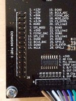
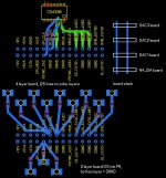
This is a sketch of the DAC boards, the stacking scheme and the possible UFL Adapter:

On top is how I'd layout the I2S connections on a DAC board to be stacked on the DSP board's header. The DAC chip is on the bottom side of a 4 layer board. MCLK line would be straight and short, SDATA lines were to be connected / disconnected by solder bridges drawn in as resistors. (I chose that way instead of possibly get made 3 particular boards, would cost 3 times more.) LRCLK and BCLK lines are routed on top side.
The DAC boards would be stacked like shown on top right, either by straight wire soldered into the pin holes or by stackable headers.
At last a raw draft of the possible UFL Adapter board.
What would you do and why would you to it?
Regards,
Gerd
These are my Options:
- Use flat ribbon cable

- Make an Adapter board an use UFL cables. Shortest i can get are 50mm long. 😕
- Stack the DAC boards onto the DSP board - desoldering the according header pins and replacing them with straight stiff wires of appropiate lenght to meet all 3 DAC boards one above the other. 😕
- As before, but using stackable pin header connectors. 😕
This is a sketch of the DAC boards, the stacking scheme and the possible UFL Adapter:
On top is how I'd layout the I2S connections on a DAC board to be stacked on the DSP board's header. The DAC chip is on the bottom side of a 4 layer board. MCLK line would be straight and short, SDATA lines were to be connected / disconnected by solder bridges drawn in as resistors. (I chose that way instead of possibly get made 3 particular boards, would cost 3 times more.) LRCLK and BCLK lines are routed on top side.
The DAC boards would be stacked like shown on top right, either by straight wire soldered into the pin holes or by stackable headers.
At last a raw draft of the possible UFL Adapter board.
What would you do and why would you to it?
Regards,
Gerd
Attachments
Last edited:
Did you test the effect for long and short or as short as possible cable ?
I've built Nos pcm1798 x2 (dddac) but separated receiver and dac board then connect them by 10cm pins cable and don't know if it is the reason of hiss noise on output...
I've built Nos pcm1798 x2 (dddac) but separated receiver and dac board then connect them by 10cm pins cable and don't know if it is the reason of hiss noise on output...
If you keep your cable shorter than Lambda/4 it does not matter which connection type you use.
Lambda is about 3 m for 100 Mhz. Its a good idea to limit the signal rise time as mutch as practical (by choosing the correct driver strength or by an external R-C filter).
Use a series resistor at the output driver to get about 1/2 Z0 to Z0 characteristic impedance match.
Hysteresis at the receiver helps too.
I see no problems at this short distances (except EMI maybe).
Hi udok,
How about the material's quality of these cable : silver, gold or bronze, which one is the best ?
How about the material's quality of these cable : silver, gold or bronze, which one is the best ?
Plain copper is the right cable material. If you like you could cover it with silver (silver has somewhat lower resistance, and due to skin effect the current is flowing in a thin surface sheet).
Bronze is a good material for connectors (spings can be made of bronze and it is resistant to corrosion).
Gold is even more resistant to corrosion and is a good coating material for low current connectors.
Z0 is about 100 ohm for ribbon cable and mutch larger for header pins (due to the larger spacings).
The reveicver chips have a high impedance. Therefore they have no big effect and you can leave them out and concentrate on one transmission line.
Source termination works by having a source impedance Rs = Z0 and no termination at the end of line.
At the DSP the driver has impedance Rs and the line has Zs. Therefore the first wave has
a voltage of Zs / (Zs + Rs). This is VCC/2 for Rs=Zs. This wave travells down to the end of
the line with about 2/3 of speed of light (20 cm / ns).
At the end of line it is reflected and the incident and reflected wave added to VCC.
The reflected wave travells to the source and is absorbed by the source impedance of Rs = Zs.
One minor problem is that the DAC receiver logic level should not be near VCC/2. The incident wave has about VCC/2 and the reflected wave has VCC.
It is not clear if the receiver switches on the incident wave.
Hysteresis at the DACs receiver helps or use a source mismatch with Rs=Zs/2
Does a handmaid soldering in the signat path, for the connectors or wires affect the quality ? (impedance, etc ?)
We saw often few pico smt caps just before the dac in those I2S signals and sometimes in front of the emitter I2S signal as well ! In case of DIY with such tweak as the OP : is there any interest to remove those caps as the big handmaid soldering add some resistance ?
Not a specialist myself but for the OP, I choosed myself to risk a connection longer than the often 10 cm advised for I2S intelinks between the emitter and receiver chips with Uf.L cables and uf-l connector on a SB Duet. Because the interest is to isolate by coax cables the I2S signal from each others, give them some insulation and match the impedance at 50 ohms between the boards. At least would use if no uf-l some mini 50 ohms coax cable (but a little too rigid... hard to do !).
But I surmise the bad soldering and the signal we hack on boards which are not designed for that to break this matched impedance. But I don't know in which proportion and how it affects the fragile signal of I2S (jitter ?).
only I2S experience i have is this : PCB path from data reader chip cca 7cm, then 0.3mm silvered copper wire without insulation, less than 1cm directly to the TDA 1453. brilliant sound, without traces of distortion / noise.
Thats no rocket science. Almost any connection with length less than 30 cm should work reliable. Only problem may be that the I2S signal is coupled to sensitive audio signals.
Two rules which help against interferences:
- add ground wires near the clock lines (gnd - clk - gnd - lrclk - gnd - rx - tx - gnd)
- limit the rise time by an R-C low pass (driver-pin -> 100p to ground -> 47R -> cable)
hand made solder joints are ok as long as they are not broken...
Two rules which help against interferences:
- add ground wires near the clock lines (gnd - clk - gnd - lrclk - gnd - rx - tx - gnd)
- limit the rise time by an R-C low pass (driver-pin -> 100p to ground -> 47R -> cable)
hand made solder joints are ok as long as they are not broken...
I thought I2S was device to device only!
When taking these signals of board (not what they were designed for) the best thing you can do is ensure that each signal always has an unbroken contiguous return path (GND). As to material, copper wire, there will be no difference using any other connector material to the signal integrity.
When taking these signals of board (not what they were designed for) the best thing you can do is ensure that each signal always has an unbroken contiguous return path (GND). As to material, copper wire, there will be no difference using any other connector material to the signal integrity.
does each signal cable from board to board needs to be isolated from each other by a coax or any standalone gnd return for the three I2S cable should be enough ?
Yes, but it's not (only) for isolation. The point is that any signal needs a return path located as close as possible to keep ground loops as small as possible.
Thank you,
so my understanding was correct (an old input by Marce)... a pity to see too much good pcbs but with only one gnd return path for all the I2S (not coax) cables...
so my understanding was correct (an old input by Marce)... a pity to see too much good pcbs but with only one gnd return path for all the I2S (not coax) cables...
The co-ax method whilst the most expensive is the best method, each signal is kept in close proximity to its return path and isolated from the other signals.
Thank you,
so my understanding was correct (an old input by Marce)... a pity to see too much good pcbs but with only one gnd return path for all the I2S (not coax) cables...
Supreme example:

😛
they will surely launch a daughter board with uf-l connectors to resolve this issue 😀, notice the longer connections than the daughter board allows solve also all the jitter issues...
Ah, a daughter boards with uf-l plugs to be connected to a standalone gnd vias motherboard as above... .... a modern poem , a fool trap 🤐... this is why after to solve this second issue you will see they launch a little sister board with a FIFO buffer to be puted between the first daughter board and the mother board 😉
off topic sorry
they will surely launch a daughter board with uf-l connectors to resolve this issue 😀, notice the longer connections than the daughter board allows solve also all the jitter issues...
Ah, a daughter boards with uf-l plugs to be connected to a standalone gnd vias motherboard as above...
.... a modern poem , a fool trap 🤐... this is why after to solve this second issue you will see they launch a little sister board with a FIFO buffer to be puted between the first daughter board and the mother board 😉off topic sorry
http://www.diyaudio.com/forums/atta...istinction-tda-1541-build-thread-imag1378.jpg
I tried to fix a "bidule"board... not sure of the quality because the hot contact between the uf-l and the pin is hard to do this way ! I have to put an uf-l plug on the Dout as well !
I tried to fix a "bidule"board... not sure of the quality because the hot contact between the uf-l and the pin is hard to do this way ! I have to put an uf-l plug on the Dout as well !
- Status
- Not open for further replies.
- Home
- Source & Line
- Digital Line Level
- I2S connection between boards - from bad to worse or how'd you do it?