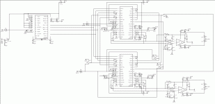
Some time ago, i wanted to buy a audio card for my PC. I've chosen the Asus Essence ST and reading about it i understand, in short, that is no good. So i started to read about DACs like MF V-DAC II and Arcam rDAC with the same result. So, i'm thinking to build my own DAC. Now, after some reading, other persons schematics analyze and copy/paste JAMBO DAC filtering stage, i've come with the attached schematics. Now, i need your help into optimizing it.
So i'll begin with some questions:
- S/PDIF connector's ground can be connected to the earth through the case without a link with the ground plane? Is needed to connect it directly to the ground plane? Can it be connected to the case who should be connected to the ground plane directly or through some passive circuit?
- Finding many different IC's configuration approaches, i'm not sure what pins can be let floating in my approach and especially on WM8741 who of them should be connected through resistors.
- I'm not sure if i need all the switches or if some of the pins should be directly set to one position not bringing me any advantage to switch (like pin 4, 25, 26) and again if them should be connected through resistors.
- I've find the signal connections between WM8804 and WM8741's very differently approached, with resistors on just two of the connections or on all of them, with resistors from 33R to 75R.
- There i have ten power supplies. Should i reduce them to four (+3.3V, +5V, +15V, -15V)?
- Not having anything in common with electronic i do not understand anything about capacitors and resistors in the filtering section. Should it be optimized? I've find some good reading about op-amp's, but for now i'm learning about PCB optimization (i have no time for all that i want and need to do, so it remains for the future).
- Is there any need for more capacitors between the power supplies and the IC'c?
Any other advice or clarification is welcomed.
Trying to complete a BOM i've find that that all the polarized capacitors will be better to be of 100uF for lower ESR. Is that okay?
Thanks.
Attachments
Last edited:
The SPDIF return needs to follow the positive signal as closely as possible, so direct to the ground plane would be best for signal integrity.
Hello, again.
Trying to draw the PCB i find myself having a simple and, whatever the answer, stupid question.
On my schematics each of the 1, 4, 5 and 6 pins of WM8804 connect to the power through 10k resistors. Can't i connect them all to the power through a single 10k resistor?
Thanks.
Trying to draw the PCB i find myself having a simple and, whatever the answer, stupid question.
On my schematics each of the 1, 4, 5 and 6 pins of WM8804 connect to the power through 10k resistors. Can't i connect them all to the power through a single 10k resistor?
Thanks.
So i'll begin with some questions:
- S/PDIF connector's ground can be connected to the earth through the case without a link with the ground plane? Is needed to connect it directly to the ground plane? Can it be connected to the case who should be connected to the ground plane directly or through some passive circuit?
The S/PDIF input will typically carry common-mode currents so if SQ is a priority do not force those interfering currents to share grounds with sensitive analog circuits. Best take the S/PDIF ground as close to the exit point for CM noise as possible. This means if you're using a transformer to power it from the mains, this will be your CM current exit point. A dedicated wire from ingress to egress is best for SQ IME.
Thank you for your answer. I understand, now, that this is not a real issue (being able to toggle between solutions at the end of the journey).
Thank you for opening my mind.
Thank you for opening my mind.
I've some more questions for you:
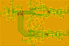
Trying to avoid vias on the signal path it's ok to have signal traces under the IC's?
How about traces under the IC's for the configuration of the IC's?
Needing to use some vias on the signal path, what of the signals should have priority on the upside of the board (LRCLK, BCLK, MCLK or digital audio signal)?
Thank you.
Hello again!
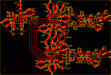
I've designed the PCB and i have numerous questions like:
- tis OK to part like that CX3 from the 14 pin of U3?
- tis OK how i placed the components on the analog signal (knowing nothing bout electronics i'm wondering if them should be placed exactly like in the schematics)?
I'll stop here with the questions, but surely i what to know everything bout the mistakes that i maded.
Thanks.
Attachments
One new question! In a few days i'll send my order, so i need your help.
I need to reduce voltage for a battery pack of 7.2V to 5.5V needed for WM8741 analog supply. I don't know the best way for this application. Voltage divider with resistors to GND, diodes, linear rectifier or what? Please help me!
I need to reduce voltage for a battery pack of 7.2V to 5.5V needed for WM8741 analog supply. I don't know the best way for this application. Voltage divider with resistors to GND, diodes, linear rectifier or what? Please help me!
- Status
- Not open for further replies.
- Home
- Source & Line
- Digital Line Level
- I need your help to build a DAC for myself - WM8804, 2*WM8741, 2*AD797