I have been working on a class D design using a cmos 4049 as the low side comparator driving npn/pnp totem pole output to IRF4214.
I am using a discrete high side driver to other IRF4214.
Specs are 1.4Mhz carrier
UCD (self oscillating design)
15uh output coil with .22uF filter capacitor
both output transistors are cool (no heat sink)
direct coupled feedback ( Av = 40)
S/n > 100db
PSRR > 85db
power supply = +- 35v
power output = 135w/ 4 ohm
Sound quality is amazing
I don't know how to measure distortion with scope but the OP275
input / feedback correction opamp is 0.0003% and no clipping is happening here.
I tried the UCC27200 driver but popped 20 fets and 10 drivers testing loading conditions and input signal overloads.
2N5401 drivers are providing amazing speed!!
Schematic
Sorry about that , I was exited that it worked.
Now I have to work on the Board component layout for
installation in the car and my old Pioneer sx3700.
3 amps, 2 channels for surround and 1 for subwoofer.
+- 40 v rails should give peaks of 250w RMS into 4 ohms.
Cheers all,
schematic
Sorry about that , I was exited that it worked.
Now I have to work on the Board component layout for
installation in the car and my old Pioneer sx3700.
3 amps, 2 channels for surround and 1 for subwoofer.
+- 40 v rails should give peaks of 250w RMS into 4 ohms.
Cheers all,
schematic
Attachments
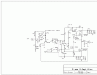
 , and where is UcD phase lead network?
And why are there both npn and pnp transistors marked 2N5401 ? and the level shifter mosfet, shouldent it go to neg rail ?
I suspect intensional errors in the schematic to make it harder for the others of us to replicate your amp.
I suspect intensional errors in the schematic to make it harder for the others of us to replicate your amp.
Errors
You are right , the Vn2010 mosfet should be on the negative rail
the NPN transistor is correctly marked as 2n4401 and PNP transistors are 2N5401.😱
You are right , the Vn2010 mosfet should be on the negative rail
the NPN transistor is correctly marked as 2n4401 and PNP transistors are 2N5401.😱
and PNP transistors are 2N5401.
.... and for the level shifter it should be vice-versa: This 2N5401 is a PNP transistor !
Regards
Charles
level shifter
The 5401 PNP level shiter is correct as the op amp (OP 275) will adjust its output level to about - 1.4v causing the voltage on the input of the 4049 to rise to about 5v. this transistor also forms a phase shift pole for self oscillation. A ramp waveform is also formed on the 4049 input.
the second feedback loop ( to OP275) has a capacitor and 4.7K resistor to improve the ramp wave output of OP275.
Cheers
It could very well be that I don't have any indepth understanding of electronics.
But I always thought that when a transistor's collector is more negative than its emitter while it is working normally - then it is almost 100% sure that it is a PNP.
Regards
Charles
But I always thought that when a transistor's collector is more negative than its emitter while it is working normally - then it is almost 100% sure that it is a PNP.
Regards
Charles
level shifter
The 5401 PNP level shifter is correct as the op amp (OP 275) will adjust its output level to about - 1.4v causing the voltage on the input of the 4049 to rise to about 5v. this transistor also forms a phase shift pole for self oscillation. A ramp waveform is also formed on the 4049 input.
the second feedback loop ( to OP275) has a capacitor and 4.7K resistor to improve the ramp wave output of OP275.
Cheers
Hi stocktrader200!
Why did you put 470 pF parallel with the lower MOSFET? Only to equalize the tpd or limit di/dt?
You can measure the THD with a good soundcard and SpectraPlus.
Why did you put 470 pF parallel with the lower MOSFET? Only to equalize the tpd or limit di/dt?
You can measure the THD with a good soundcard and SpectraPlus.
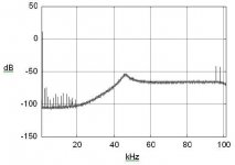
My FPGA-based post-filter fed-back and PSV fed-forward digital Class-D can do 0.05 % to 4 Ohm and 0.02 % unloaded (fig.) at 1 kHz, with TAS5261 and wall wire winded MPP inductors.  I'm very excited about yours. 🙂
I would patent mine. Does anybody know how to do it?
I'm very excited about yours. 🙂I would patent mine. Does anybody know how to do it?
Attachments
response
I can't believe the response that this circuit has generated.
I will be selling a Stereo 4 layer main board of this layout shortly on ebay as I have no website.
The 470 pf capacitor is to counteract stray parasitic capacitances in the output mosfet that could turn on the device as the output transitions from low to high.
The testing I have been doing states it may not be necessary.
I will put that information on the updated schematic.
Cheers,
Steve
- Status
- Not open for further replies.
- Home
- Amplifiers
- Class D
- I got My class D working !!