This is a simulation of IPS and VAS circuit similar to Apexaudio SR200. I cannot get reasonable result. It is strange. Attached is the file, I cannot see what I did wrong.
I did a few other circuits and never ran into problem. I even uninstalled and reinstalled the LTSpice to make sure nothing wrong with the program. Please help.
Thanks
I did a few other circuits and never ran into problem. I even uninstalled and reinstalled the LTSpice to make sure nothing wrong with the program. Please help.
Thanks
Attachments
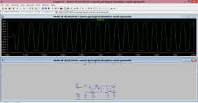
I don't see it. I measure every single voltage of the voltage sources and trace the circuit. The current is not right. I cut the AC generator and measure all the voltage and current a few times already before a post. If you measure current through R3 is 1.8mA. BUT if yo measure current through R4 and R5, it's 0.2mA. the whole thing does not make sense. Q6 and Q7 is not going to pull so much current through the base!! I change transistors, nothing make sense. This circuit is very similar to the Apexaudio SR200 front end.
BTW, thanks for the thread that you made in showing how to run simulation with LTSpice. I learn how to do FFT from your posts. I did a few different circuit simulations today and all came out......until this one!!!! Please help.
Thanks
BTW, thanks for the thread that you made in showing how to run simulation with LTSpice. I learn how to do FFT from your posts. I did a few different circuit simulations today and all came out......until this one!!!! Please help.
Thanks
Last edited:
Pleased you are finding the LT thread useful.
Look at the DC voltages on Q8 and Q9. What is on the base of the two devices. Where is that voltage derived from ?
If this were a real circuit on a real PCB the fault would be open circuit print.
Look at the DC voltages on Q8 and Q9. What is on the base of the two devices. Where is that voltage derived from ?
If this were a real circuit on a real PCB the fault would be open circuit print.
The base of Q8 and Q9 is 4V below +40V which is 36V. Why are the voltages at the collector of Q6 and Q7 is around 39V? It should be 36.7V governed by the emitter of Q8 and Q9.
I measure the voltages and current so so many times already!!! Current through R3 at the bottom of the IPS is 1.8mA. BUT current through R4 and R5 is only 0.2mA. Where's the current gone? Current through R4 and R5 should summed to almost 1.8mA!!! Nothing make sense. That's why I reinstalled the program just to make sure.
I measured current through R6 and R7, R6 is about 1.6mA, R7 is low. So Q6 and Q7 does not draw much base current. So where does the current from R3 goes? I measure all the DC voltage sources at the connections of the circuit to make sure I got the wires connected.
This circuit should work in real life like Apexaudio amplifier. I worked on it for over 3 hours before I posted. I must have a blind spot looking at the schematic and I don't think I will see it anymore. If you see the problem, please let me know.
Your thread is very good, I hate to read through the help file and instructions as they never get to the point. It is so much faster to follow your thread. I only got through the FFT plotting, still have more to go before I am stuck on this one. Actually I simulate this one as an exercise, never thought I got stuck. I did few of the full symmetric IPS VAS that almost double the complexity, worked out just perfect and get the result. Just want to do the Apexaudio for the fun of it to see why it is so good.
Last edited:
The base of Q8 and Q9 is 4V below +40V which is 36V.
Measure it again 🙂 Don't assume anything... measure on the base of each transistor.
I did, every time you tell me, I did. I measured every point around Q8 and Q9. It does not make sense. In real circuit, I'll be looking a solder bridge!!!
When base of Q8 and Q9 is at 36V, the emitters cannot at 39V. That's a tell tale something is really wrong of the circuit already.
Please tell me what I did wrong if you see it. I don't even know how many times I measured all the notes......every single wires already before I posted. That's the reason I spent more time typing now.
Last edited:
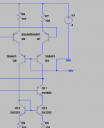
You should take more care when you wire up sims. Draw the circuit so that every connection is shown explicitly. Don't run one wire on top of another to get to the connection point, this is just lazy, sloppy and leads to errors.
Maybe you are right, I change the wires and looks different.You should take more care when you wire up sims. Draw the circuit so that every connection is shown explicitly. Don't run one wire on top of another to get to the connection point, this is just lazy, sloppy and leads to errors.
Last edited:
I don't understand why the wire through the base of the transistor makes a difference. I have been simulating like that all along and have no problem. I went back and change the other simulation files, it did not make a dent of a difference, only this one.
But anyway, thanks for the time.
But anyway, thanks for the time.
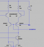
I did check and read the same!!! It was strange. I went in the wires are read!!!So this is what you had and what it should have been. Not obvious at all to look at the diagram but the voltage checks showed the problem in seconds.
BTW, how do you get the display of voltage, I did not see you showing that. You just mentioned you can display the voltage. I did follow you on labeling the notes, but not displaying the voltage. I have to keep reading off the graph.
Last edited:
If you run the sim and hover the cursor to the left of Q9 you read 39 volts. Move to the right and its 36. Although the trace wire looks continuous it obviously isn't, it not being connected to Q9 base.
I did check and read the same!!! It was strange. I went in the wires are read!!!
BTW, how do you get the display of voltage, I did not see you showing that. You just mentioned you can display the voltage. I did follow you on labeling the notes, but not displaying the voltage. I have to keep reading off the graph.
Two ways. Run the sim and hover the cursor over any point and the voltage is displayed at the lower left of the screen. That works for both transient sims (as yours is set up) or just a DC operating point sim (alter the edit simulation to DC op pnt). Once you run a simple DC op point then you can click on any point on the diagram and the voltage at that point attaches to the schematic. Change a part and re-run and the voltages change and display automatically.
I don't see any frequency compensation components anywhere; there is a pretty good chance the amplifier may not be stable. It may oscillate in simulation. It may oscillate at 9.94 megahertz in simulation..
Read post #16 here on how to attach voltages,
http://www.diyaudio.com/forums/soft...ng-ltspice-beginner-advanced.html#post4030525
http://www.diyaudio.com/forums/soft...ng-ltspice-beginner-advanced.html#post4030525
Two ways. Run the sim and hover the cursor over any point and the voltage is displayed at the lower left of the screen. That works for both transient sims (as yours is set up) or just a DC operating point sim (alter the edit simulation to DC op pnt). Once you run a simple DC op point then you can click on any point on the diagram and the voltage at that point attaches to the schematic. Change a part and re-run and the voltages change and display automatically.
Thank you so very much. I got it. If I know to hover around and read from the lower left of the screen, I would have found the problem!!!
Thanks
Last edited:
And also, it (the connection between Q8 and Q9) doesn't have that little square dot that tells you "three things are connected together here" as it does in between (for a very similar example) Q3 and Q4.
In addition to measuring the voltages, if you use the Drag tool to move Q8 and Q9 around, the mistake will become obvious.
I like the base connections at (for examples) Q1 and Q2 much better than those others and Q5 (where a wire connecting the base goes through the transistor). I'd been doing these things perhaps semi-unconsciously in LTspice (and other but nicer schematic capture interfaces), but this certainly points out why. If you connect three things, make one at 90 degrees to the other two, and make sure there's a square dot where all three meet.
Sometimes (ahem...) things don't have a great "user interface," and it's up to the poor user to develop defensive rules to make up for it and help avoid Gotcha's like this.
It almost sounds like the participants in this thread are unaware of the LTSPICE error log ??
After running a simulation you can click View -> SPICE Error Log (or, you can simply type the keyboard shortcut Ctrl+L). In this case it tells you exactly where the problem is.
_
After running a simulation you can click View -> SPICE Error Log (or, you can simply type the keyboard shortcut Ctrl+L). In this case it tells you exactly where the problem is.
_
Attachments

- Status
- Not open for further replies.
- Home
- Design & Build
- Software Tools
- I cannot get a logical simulation result on this