Along the years, I have accumulated a number of ideas, circuits, topologies, etc., and withheld the ones that had no immediate use, in the hope of using them later, patenting some, etc.
Since this will not happen now, I prefer to release them for the benefit of the community, and make them public rather than let them go to waste.
Many of them have no direct relationship with audio (but who knows?), which is why this is posted in "Everything else".
They are completely free to use, by anyone, for any purpose: you can use them as you like, even commercially, and you do not even need to acknowledge the origin: the concept could be hidden inside a product without anyone knowing but you: absolute public domain, totally unrestricted.
What you cannot do is restrict the public domain, by claiming it is your invention or IP, patenting it, etc. They have to remain available for all, without restriction.
If you devise a significant improvement based on them, you have the right to claim the IP as yours for that aspect, but it is something I discourage: please remain in the spirit of this thread, and offer your own contribution to the community.
I have no realistic way of enforcing those conditions, but plunderers beware: the DIY community is extremely vigilant, and they will contest any tentative of sneaky appropriation (I had an occasion to see that vigilance in action).
If you notice a material error, please mention it. Chances are low, because most have been tested in some way, but one is never 100% certain.
These ideas are offered for what they are worth, and they are free, so no need to complain: if you don't like them, ignore them and move along...
The first concept is a logarithmic, current-mode, AD converter. A bit outlandish at first sight, but it makes sense in the right context.
This converter takes a current as an input, and converts it into a digital value representing the logarithm of the current.
This is useful in optical power measurement: the front-end of the instrument typically delivers a current proportional to the incident power (a photodiode), and due to the large dynamic range, the output is displayed as dB.
Optical measurements have a particular quirk: the photo-current is proportional to the incident optical power. This means that in order to cover 80dB, which is reasonable for an ordinary power-meter, you need to cover a 160dB current range, which is not exactly trivial.
The standard solution nowadays would involve a precision opamp operating as a TIA, followed by a very high resolution AD converter and digital processing to display the dB value relative to 1mW.
It is however possible to dispense with the heavy artillery.
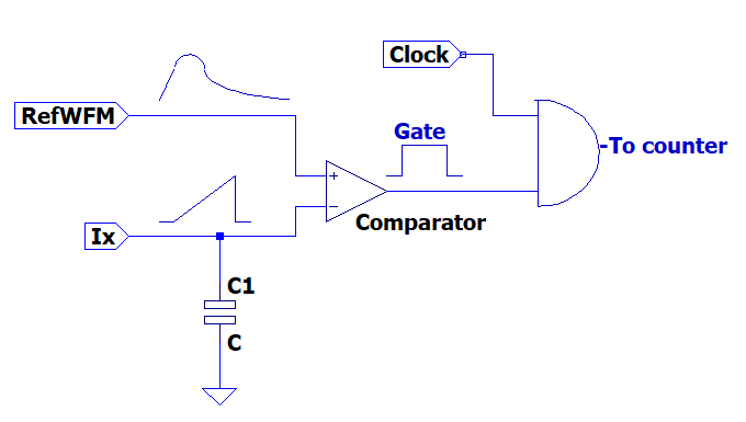
You can integrate the current with a simple capacitor, and compare the resulting voltage ramp to a suitable reference waveform. This will generate a gating window, proportional to the logarithm of the current. Converting a time period into a digital form is then the easiest thing to do.
Feeding the unknown current directly into an integrator has a number of advantages: a current can cover many decades without being affected by thermoelectric voltages, and the integrator has an inherent low-pass behaviour, helping to filter the noise.
The slope-based nature of the converter lends itself to auto-zero and offset elimination: switches are needed anyway to reset the integrator(s).
In its simplified form, the circuit would look like this:
Now, we have to find a suitable reference waveform. We want the intercept point t=log i (dropping all the constants required for units consistency, etc)
As i=cu/t, t=log cu/t.
In fact the slope is inverted: the time increases when the current decreases: an inversion or a negative sign in front of the log is required: t=-ln cu/t
Take the exponential of both sides e^(-t)=cu/t, and u=t e^(-t), dropping another constant.
The bare-bone function looks like this (blue):
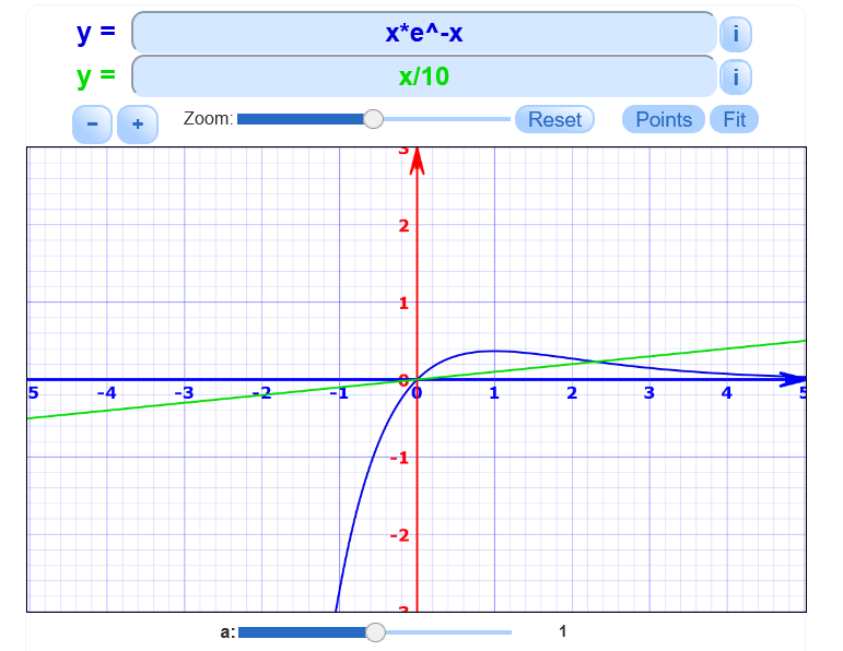
The green is the ramp generated by the integrator (this is the graphing tool: https://www.mathsisfun.com/data/fun...xmin=-5.029&xmax=5.029&ymin=-3.000&ymax=3.000)
How can you generate the reference waveform? It is extremely simple, you just need to integrate and differentiate a step using passive, RC circuits, with a buffer in-between.
The order doesn't matter, but it may impact the performance: with the integrator last, the waveform will be filtered, but the offset of the buffer will be present. With the differentiator last, no offset, but the noise will be unattenuated.
This sim illustrates the concept in its most basic form, with spice building blocks.
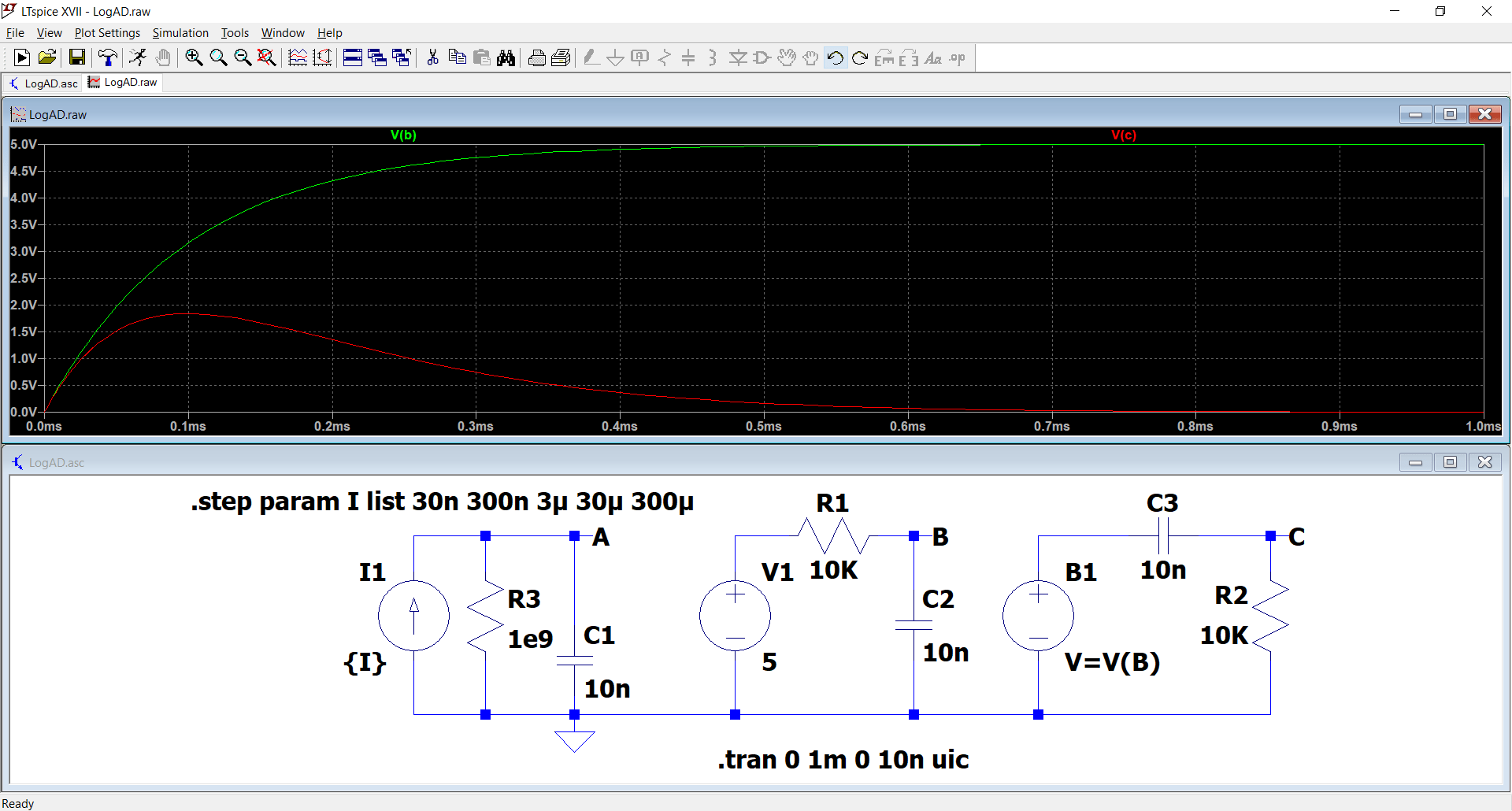
B is the output of the passive integrator after the step, and C the final output.
This pic shows the waveform with various slopes, decades apart:
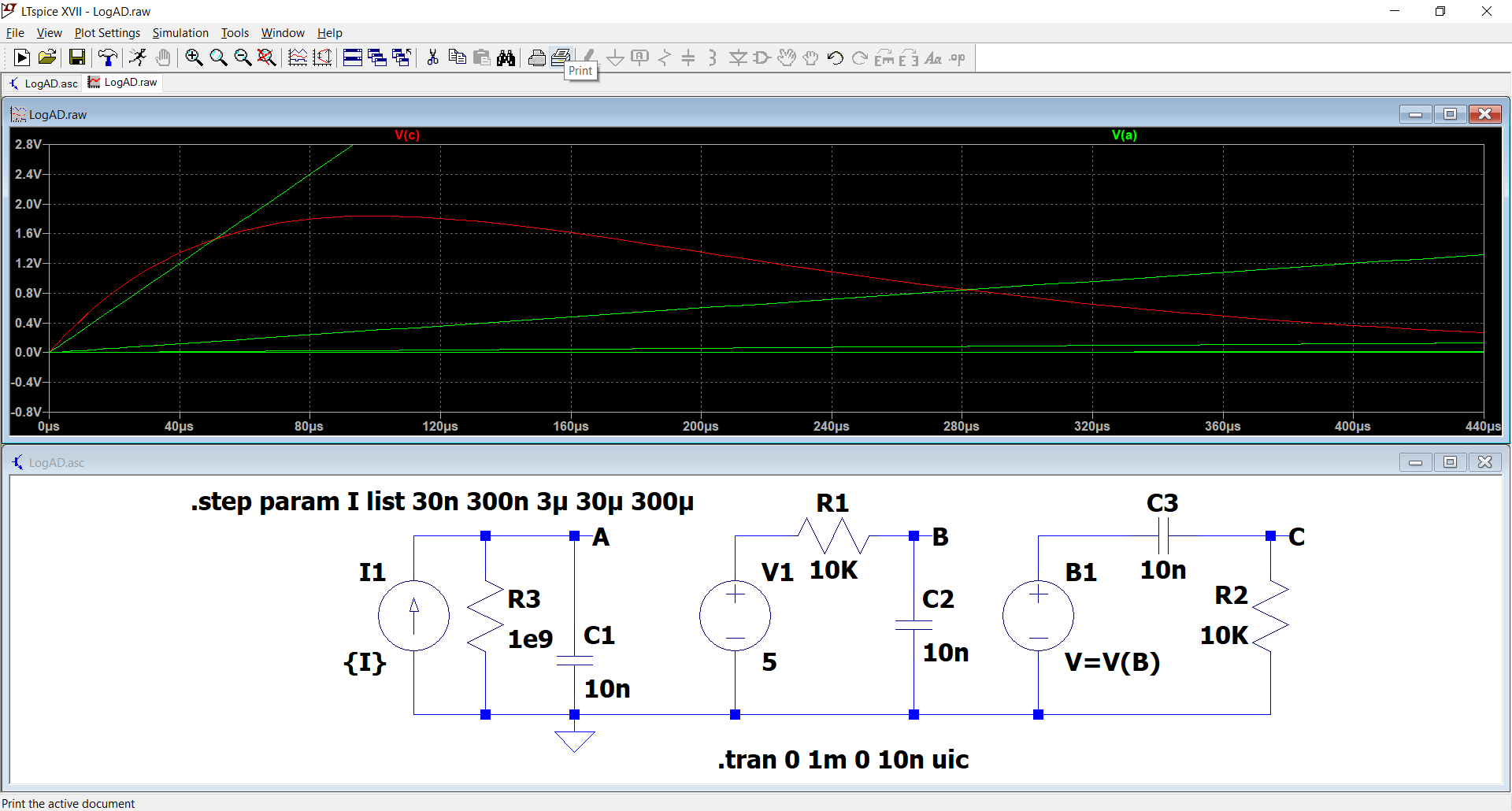
It is not very legible in linear mode; this is the same in log mode:
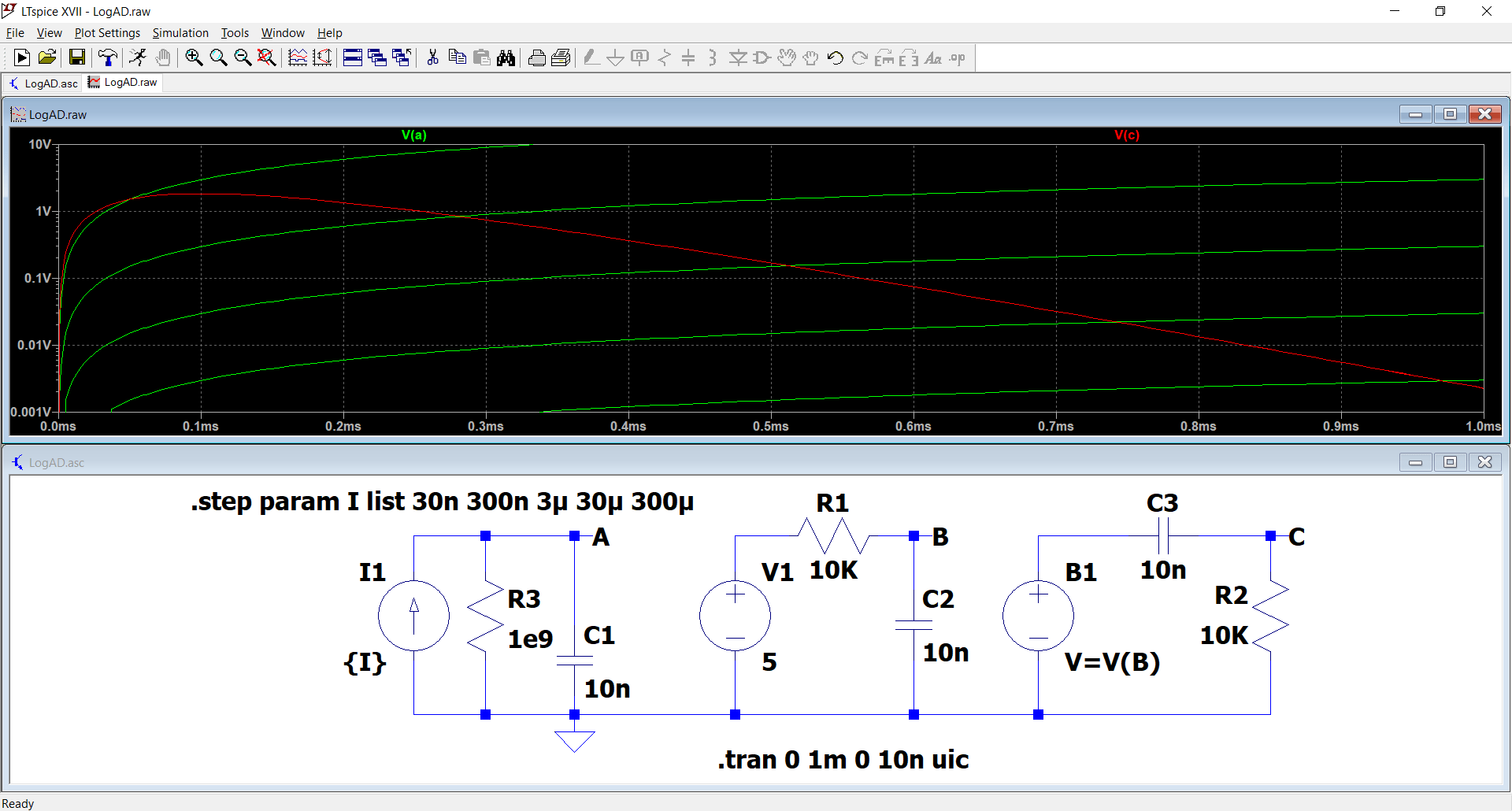
It becomes clear that the intercept points for each decade are separated by the same time interval. This shows that the scheme is functional.
It has its issues, of course: nothing is perfect. For example, the integrator's slope cannot be steeper than the reference waveform at the origin.
When you go deeper in the -dB region, the comparator needs to resolve small voltages, but that is something slope-based converters have become very good at.
You need to do your homework, and compute all the constants according to your application: I only show the fundamental principles, not the gory details, but it can be made to work, and very effectively.
I post the sim file, and if you want the log display, you need to reload the plot setting
Since this will not happen now, I prefer to release them for the benefit of the community, and make them public rather than let them go to waste.
Many of them have no direct relationship with audio (but who knows?), which is why this is posted in "Everything else".
They are completely free to use, by anyone, for any purpose: you can use them as you like, even commercially, and you do not even need to acknowledge the origin: the concept could be hidden inside a product without anyone knowing but you: absolute public domain, totally unrestricted.
What you cannot do is restrict the public domain, by claiming it is your invention or IP, patenting it, etc. They have to remain available for all, without restriction.
If you devise a significant improvement based on them, you have the right to claim the IP as yours for that aspect, but it is something I discourage: please remain in the spirit of this thread, and offer your own contribution to the community.
I have no realistic way of enforcing those conditions, but plunderers beware: the DIY community is extremely vigilant, and they will contest any tentative of sneaky appropriation (I had an occasion to see that vigilance in action).
If you notice a material error, please mention it. Chances are low, because most have been tested in some way, but one is never 100% certain.
These ideas are offered for what they are worth, and they are free, so no need to complain: if you don't like them, ignore them and move along...
The first concept is a logarithmic, current-mode, AD converter. A bit outlandish at first sight, but it makes sense in the right context.
This converter takes a current as an input, and converts it into a digital value representing the logarithm of the current.
This is useful in optical power measurement: the front-end of the instrument typically delivers a current proportional to the incident power (a photodiode), and due to the large dynamic range, the output is displayed as dB.
Optical measurements have a particular quirk: the photo-current is proportional to the incident optical power. This means that in order to cover 80dB, which is reasonable for an ordinary power-meter, you need to cover a 160dB current range, which is not exactly trivial.
The standard solution nowadays would involve a precision opamp operating as a TIA, followed by a very high resolution AD converter and digital processing to display the dB value relative to 1mW.
It is however possible to dispense with the heavy artillery.
You can integrate the current with a simple capacitor, and compare the resulting voltage ramp to a suitable reference waveform. This will generate a gating window, proportional to the logarithm of the current. Converting a time period into a digital form is then the easiest thing to do.
Feeding the unknown current directly into an integrator has a number of advantages: a current can cover many decades without being affected by thermoelectric voltages, and the integrator has an inherent low-pass behaviour, helping to filter the noise.
The slope-based nature of the converter lends itself to auto-zero and offset elimination: switches are needed anyway to reset the integrator(s).
In its simplified form, the circuit would look like this:
Now, we have to find a suitable reference waveform. We want the intercept point t=log i (dropping all the constants required for units consistency, etc)
As i=cu/t, t=log cu/t.
In fact the slope is inverted: the time increases when the current decreases: an inversion or a negative sign in front of the log is required: t=-ln cu/t
Take the exponential of both sides e^(-t)=cu/t, and u=t e^(-t), dropping another constant.
The bare-bone function looks like this (blue):
The green is the ramp generated by the integrator (this is the graphing tool: https://www.mathsisfun.com/data/fun...xmin=-5.029&xmax=5.029&ymin=-3.000&ymax=3.000)
How can you generate the reference waveform? It is extremely simple, you just need to integrate and differentiate a step using passive, RC circuits, with a buffer in-between.
The order doesn't matter, but it may impact the performance: with the integrator last, the waveform will be filtered, but the offset of the buffer will be present. With the differentiator last, no offset, but the noise will be unattenuated.
This sim illustrates the concept in its most basic form, with spice building blocks.
B is the output of the passive integrator after the step, and C the final output.
This pic shows the waveform with various slopes, decades apart:
It is not very legible in linear mode; this is the same in log mode:
It becomes clear that the intercept points for each decade are separated by the same time interval. This shows that the scheme is functional.
It has its issues, of course: nothing is perfect. For example, the integrator's slope cannot be steeper than the reference waveform at the origin.
When you go deeper in the -dB region, the comparator needs to resolve small voltages, but that is something slope-based converters have become very good at.
You need to do your homework, and compute all the constants according to your application: I only show the fundamental principles, not the gory details, but it can be made to work, and very effectively.
I post the sim file, and if you want the log display, you need to reload the plot setting
Attachments
This scheme has actually been tested: I have worked for years in an optical lab, and among the many instruments, optical attenuators were ubiquitous. They ranged from the simplest mechanical/optical ones to the most sophisticated, electronic, GPIB controllable types.
One of our workhorse was based on a movable wedge, mechanically controlled from the front panel via gears. A potentiometer was also linked to the system, to monitor the position. The voltage from the potentiometer was processed to compensate for the various imperfections, and convert the position into dB's for display.
It was powered by a large, non-rechargeable lithium battery pack.
One day, the batteries started to fail: they had been in use for years. Unfortunately, the main battery was the only one, and had no backup. This meant that when the battery failed, the translation data stored in CMOS RAM was lost, rendering the instrument useless, even after the battery had been replaced.
The only solution was to send them back to the factory, in Canada for battery replacement and recreation of the translation data, probably on a special test and calibration bench.
It would have been costly, required lots of paperwork for the temporary export, etc. and in addition it would have had to be done again later, when the replacement batteries die.
It was more advantageous to scrap the whole lot, and buy new ones. It was a pity, because apart from that flaw, they were good instruments, convenient and portable thanks to the battery operation.
I took on my own time to try to save them, and I noticed that the optical wedge was large enough to accommodate additional components. We had quite a number of obsolete 1310nm lasers and photodiodes, and I could install them on each side of the wedge, to monitor the actual attenuation. I needed to translate the attenuation in dB, to send it to the display.
This is how I devised the circuit: it could work in pulse mode, at a low duty-cycle, like 1ms activity every second to save power, and I could calibrate it to display the correct value.
For the user, the modification was completely transparent: the instrument worked exactly as before, and was even more accurate, because the displayed value was actually measured, not deducted from the mechanical position. The batteries were now ordinary AA's, and replaceable without problem.
I proposed the mod to the head of the labs, and he was quite pleased with it, and I went on to modify the whole lot. The boss was a typical bean-counter, totally uninterested in the technical details: he was just seeing the economy of a few thousand euros, and the time and paperwork saving. Nobody ever asked me how I had done it, they just continued to use the attenuators as they always did....
Next, The Gainuator:
But first, one more word about the previous subject: I mentioned optical measurements as an application, but the concept can probably be used in other fields, like nuclear physics for example.
Back to the gainuator: ever wondered how an attenuator built from negative resistors would behave?
Here is the answer: all four circuits are ~10dB attenuators, built for a 100ohm characteristic impedance. Some are in the T format and other in the PI one. The two bottom ones use negative resistors, something allowed by spice simulators.
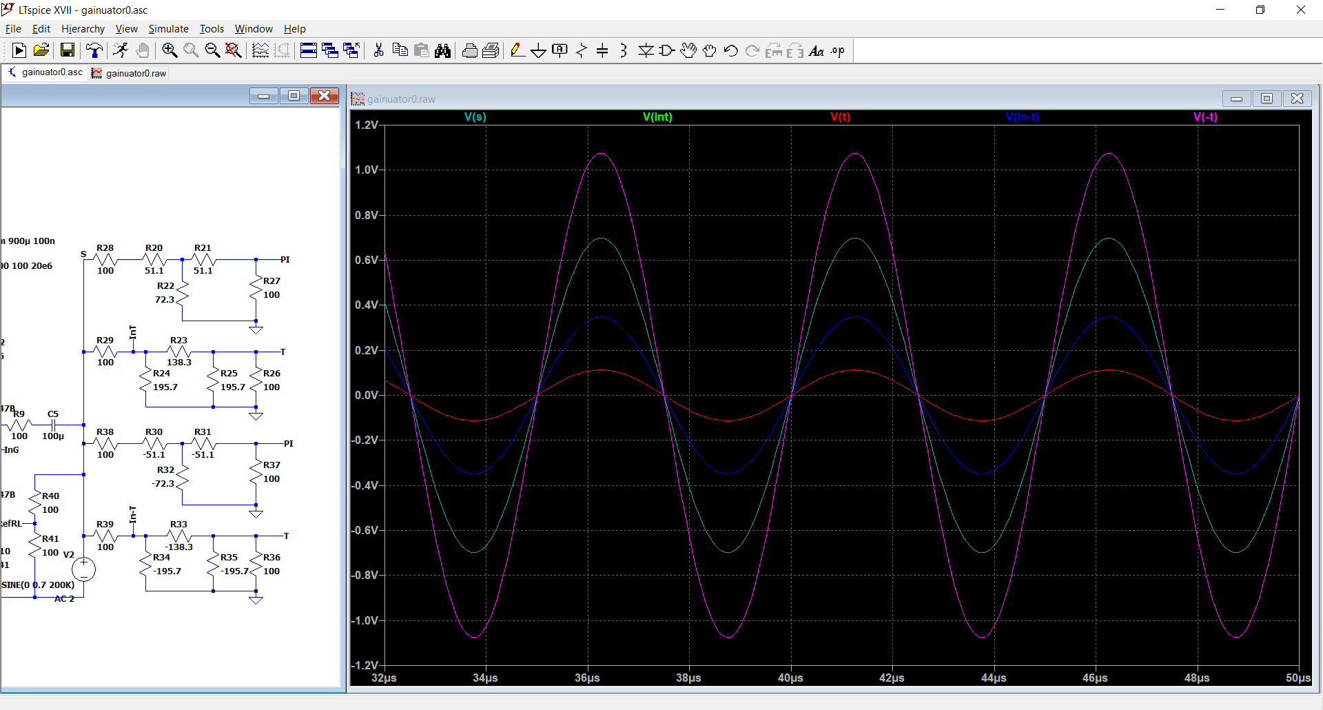
You might think that it would be unstable or unpredictable. Not at all: trace S (cyan) is the source, traces InT and In-T show the signal after the input matching resistors (blue and green traces superposed), and the red and magenta traces are the outputs of the regular and negative T attenuators, respectively.
As expected, the red trace is 10dB down, but the magenta is 10dB up.
This means that the input impedance of the negative attenuator is real and positive (blue and green traces are undistinguishable), and instead of an attenuation it provides an amplification.
This can be demonstrated by computing the values of the characteristic impedance and attenuation for negative components.
This means that this negative attenuator is in fact an amplifier. Nothing to write home about: there are many ways of building an amplifier, using less exotic methods. But this one is completely symmetrical, and therefore bilateral: input and output are completely exchangeable.
This becomes more interesting, but bilateral amplifiers or repeaters already exist: they are typically made from two distinct amplifiers and two directional bridges to separate and recombine the Rx and Tx directions.
Anyway, such a negative attenuator is completely hypothetical and chimerical, and could never exist outside of a simulator or the mind of a deranged electronician. Or could it?
Let's look at this circuit:
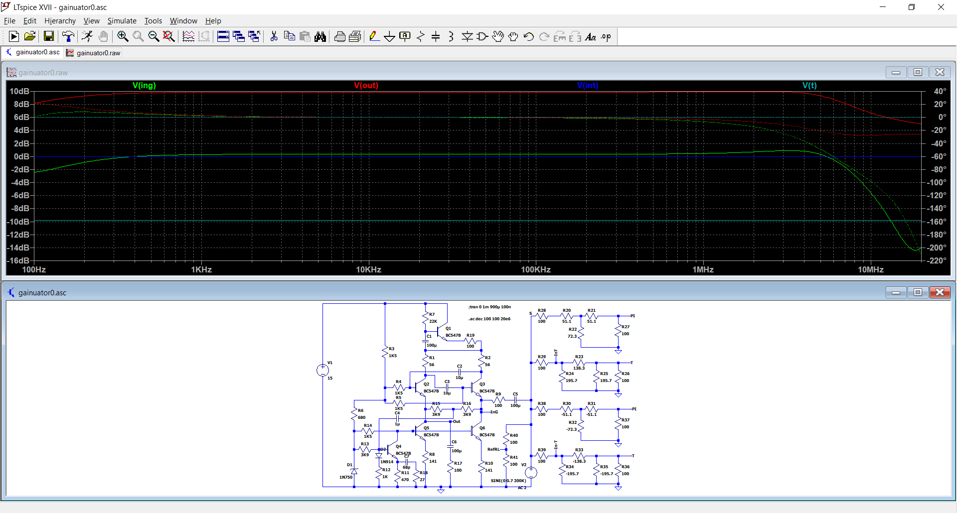
InG and InT are practically identical (green & blue), meaning the input impedance of the "Gainuator" is 100ohm, just like the regular attenuator, but the outputs (red and cyan) are 20dB apart: +10 and -10.
This means that this circuit actually behaves like a negative attenuator.
The actual configuration is difficult to classify: it is mostly a PI configuration, but with a hint of T. There is a middle, floating negative resistor, but the shunt parts are made from two negative resistors fed from a T center point. It is thus a kind of hybrid, but the important thing is that it actually works.... In sim at least. It could be pie in the sky.
Not really:
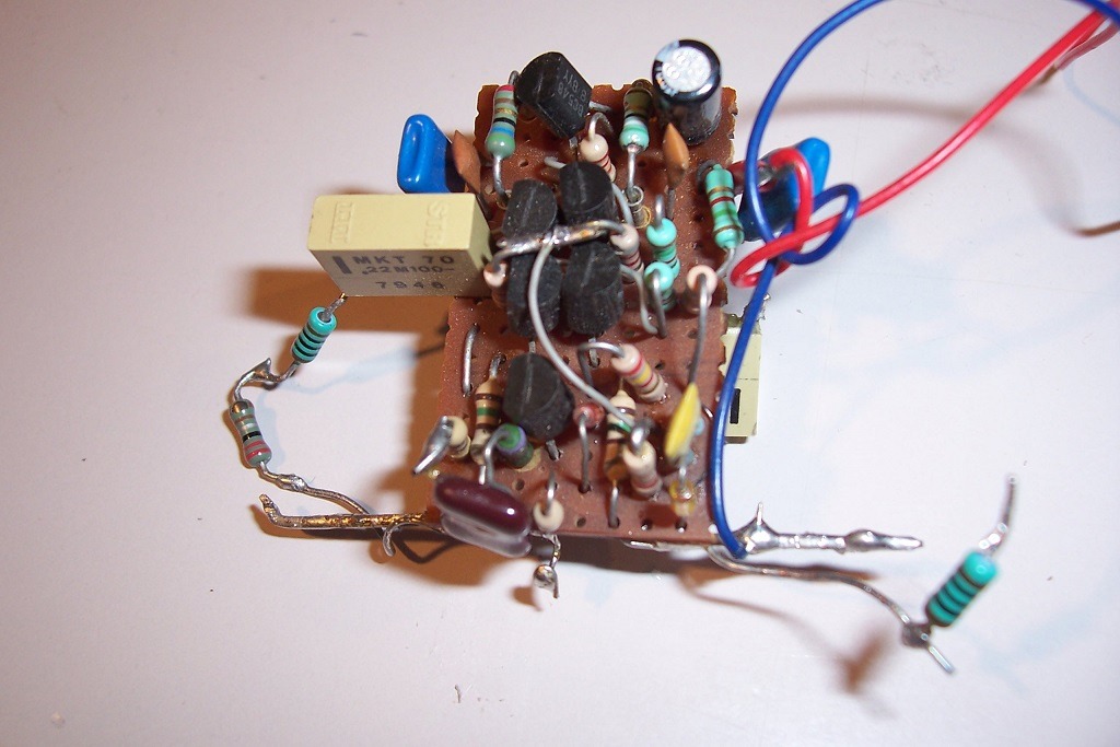
This has actually been built and tested as a bilateral repeater for DSL signals.
Note that the concept of negative resistors is not new in the field of telecommunications: repeaters made from "negistors" have been developed, but they could only be used for minor gain corrections, because the negative resistor changed the characteristic impedance and degraded the return loss.
The concept of a complete negative attenuator addresses this issue, and remains simpler than all the hardware required by two separate amplifiers and coupling circuits.
But first, one more word about the previous subject: I mentioned optical measurements as an application, but the concept can probably be used in other fields, like nuclear physics for example.
Back to the gainuator: ever wondered how an attenuator built from negative resistors would behave?
Here is the answer: all four circuits are ~10dB attenuators, built for a 100ohm characteristic impedance. Some are in the T format and other in the PI one. The two bottom ones use negative resistors, something allowed by spice simulators.
You might think that it would be unstable or unpredictable. Not at all: trace S (cyan) is the source, traces InT and In-T show the signal after the input matching resistors (blue and green traces superposed), and the red and magenta traces are the outputs of the regular and negative T attenuators, respectively.
As expected, the red trace is 10dB down, but the magenta is 10dB up.
This means that the input impedance of the negative attenuator is real and positive (blue and green traces are undistinguishable), and instead of an attenuation it provides an amplification.
This can be demonstrated by computing the values of the characteristic impedance and attenuation for negative components.
This means that this negative attenuator is in fact an amplifier. Nothing to write home about: there are many ways of building an amplifier, using less exotic methods. But this one is completely symmetrical, and therefore bilateral: input and output are completely exchangeable.
This becomes more interesting, but bilateral amplifiers or repeaters already exist: they are typically made from two distinct amplifiers and two directional bridges to separate and recombine the Rx and Tx directions.
Anyway, such a negative attenuator is completely hypothetical and chimerical, and could never exist outside of a simulator or the mind of a deranged electronician. Or could it?
Let's look at this circuit:
InG and InT are practically identical (green & blue), meaning the input impedance of the "Gainuator" is 100ohm, just like the regular attenuator, but the outputs (red and cyan) are 20dB apart: +10 and -10.
This means that this circuit actually behaves like a negative attenuator.
The actual configuration is difficult to classify: it is mostly a PI configuration, but with a hint of T. There is a middle, floating negative resistor, but the shunt parts are made from two negative resistors fed from a T center point. It is thus a kind of hybrid, but the important thing is that it actually works.... In sim at least. It could be pie in the sky.
Not really:
This has actually been built and tested as a bilateral repeater for DSL signals.
Note that the concept of negative resistors is not new in the field of telecommunications: repeaters made from "negistors" have been developed, but they could only be used for minor gain corrections, because the negative resistor changed the characteristic impedance and degraded the return loss.
The concept of a complete negative attenuator addresses this issue, and remains simpler than all the hardware required by two separate amplifiers and coupling circuits.
Attachments
Long ago, neg-R bi-di repeaters were developed, and occasionally deployed, to extend the reach of POTS voice telephone. As you suggest, for large gain, by the time you compensate all the interactions, you might as well get a fatter wire.This has actually been built and tested as a bilateral repeater for DSL signals.
https://patents.google.com/patent/US2904641
https://patents.google.com/patent/US3814866
Here is a short description of the circuit:
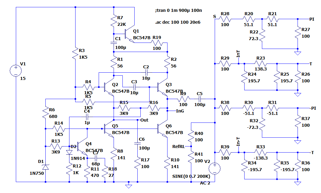
The cross-coupled Q2 & Q3 synthesize the series resistor of the PI attenuator (the analogue of R33 in the simulated version). They need to see an impedance in their emitters in order to achieve that.
The impedance is formed by the I/O lines, and two other synthetic negative resistors generated by Q5 and Q6, with the help of Q5 which amplifies and inverts the average of the I/O ports thanks to R15 & 16.
The two inversions result in a positive feedback, causing the negative resistance behaviour.
In order to keep the series negative resistor floating, the whole circuit is fed by a gyrator built around Q1.
The circuit is far from perfect in its implementation, mainly because of the need to include resistors to bias the transistors. These parasitic resistors somewhat upset the ideal synthesis of the gainuator.
This can be seen in the return loss figure: -27.5dB at best, against -77dB for the purely synthetic one
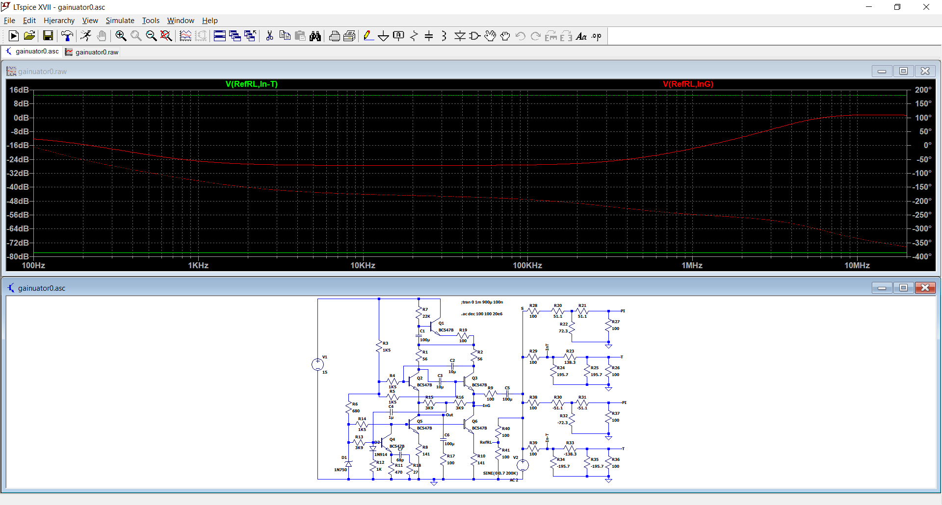
That said, anything better than -25dB is deemed excellent in real life, and the circuit could be refined further. It is probably even possible to use the circuit itself to cancel its own parasitics, but that would require some brain-twisting exercises.
This is far from the only possible implementation: this time a purely PI type, with no hint of T present:
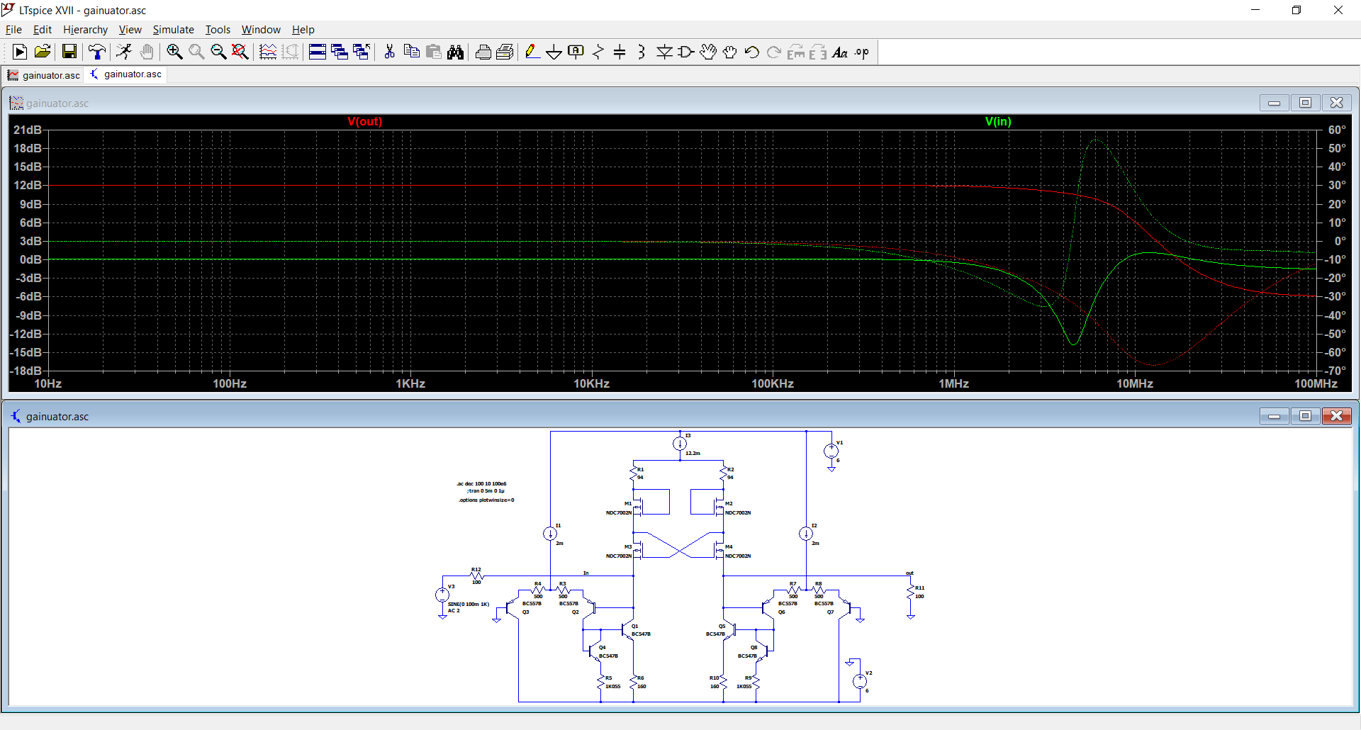
The cross-coupled Q2 & Q3 synthesize the series resistor of the PI attenuator (the analogue of R33 in the simulated version). They need to see an impedance in their emitters in order to achieve that.
The impedance is formed by the I/O lines, and two other synthetic negative resistors generated by Q5 and Q6, with the help of Q5 which amplifies and inverts the average of the I/O ports thanks to R15 & 16.
The two inversions result in a positive feedback, causing the negative resistance behaviour.
In order to keep the series negative resistor floating, the whole circuit is fed by a gyrator built around Q1.
The circuit is far from perfect in its implementation, mainly because of the need to include resistors to bias the transistors. These parasitic resistors somewhat upset the ideal synthesis of the gainuator.
This can be seen in the return loss figure: -27.5dB at best, against -77dB for the purely synthetic one
That said, anything better than -25dB is deemed excellent in real life, and the circuit could be refined further. It is probably even possible to use the circuit itself to cancel its own parasitics, but that would require some brain-twisting exercises.
This is far from the only possible implementation: this time a purely PI type, with no hint of T present:
Attachments
Fractional voltage multipliers
The front of "traditional" voltage multipliers has been extremely quiet for years, decades, and even a whole century: all of the major topologies like Greinacher, Schenkel, Latour, Delon, Villard, Cockcroft, Dickson, etc. have been invented ~100 years ago or more. There have been minor topology changes for some, like a different connection of capacitors, but the base structure remained the same.
By "traditional", I mean those based on autonomous switching elements, ie. diodes, capable of deciding by themselves when to conduct and when to block, based on the polarity they see.
The arrival of practical controlled switches in the seventies revolutionized the field, allowing charge pumps to work as step-down or fractional converters.
However, there is a tacit, implicit comprehension that traditional multipliers are unable to perform such acrobatics, and that they are limited to a multiplication by n, with n being any integer, thereby ruling out fractional multipliers and step-down converters since the only integer value <1 is 0, which is possible of course, but not extra-useful in practice.
Tentatives have been made with quirky circuits that appear to work as fractional converters under very special conditions, but in practice they are just topologies having high, concentrated losses for their theoretical voltage, regressing to a lower order multiplication ratio as soon as they see a significant load. This means a high internal resistance, heavy losses and heavy stresses on one or two components.
In short, they are a cheat, and don't really qualify.
Thus, there seems to be no hope, and the traditional view seems to hold, even though there is no actual demonstration that a fractional multiplier is impossible.
Is it really the case?
No.
And here is the proof:
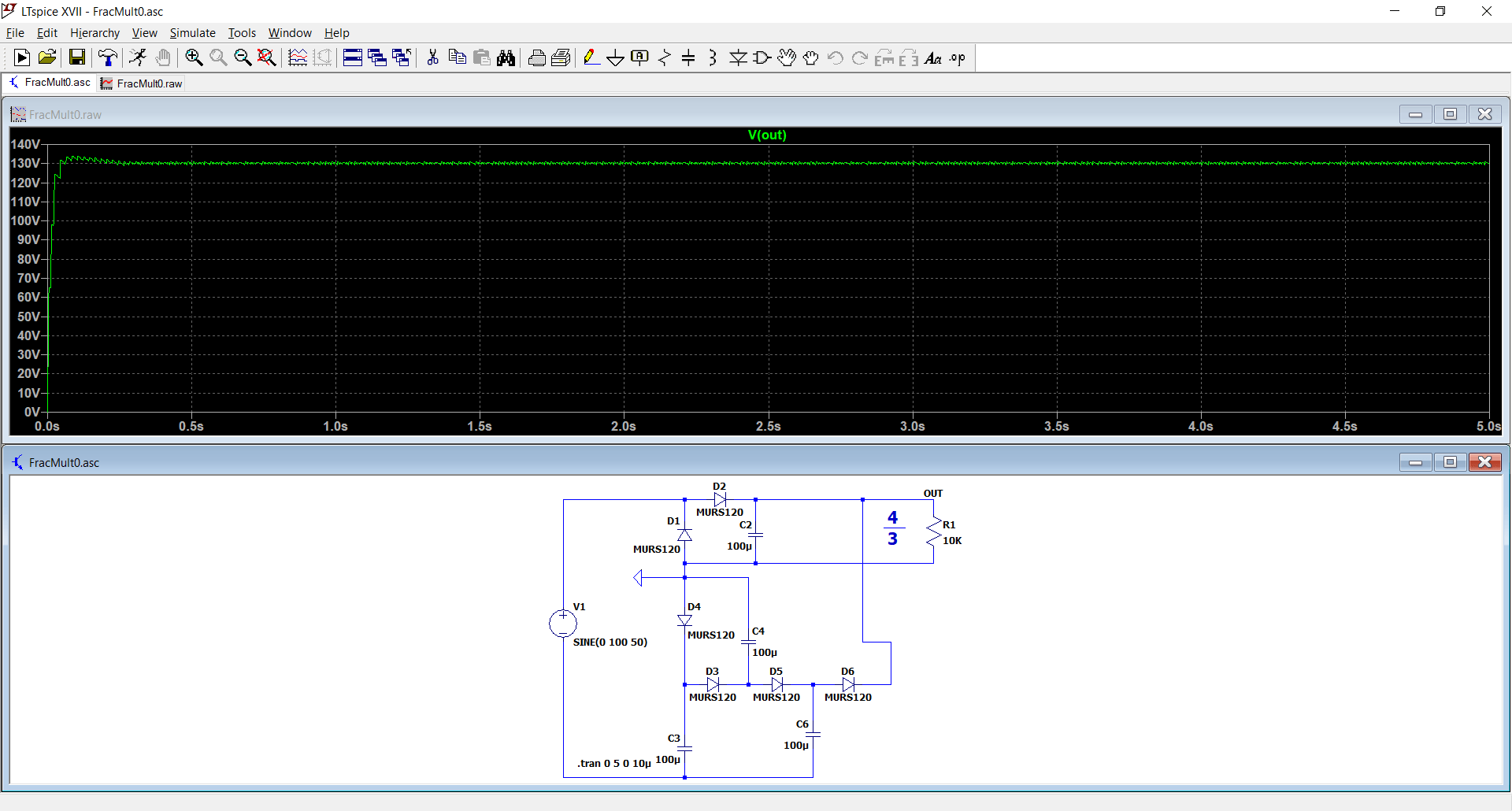
It is a working example of 4/3rd multiplier (I can see some of you frantically typing, trying to find a precedent, but I don't think it will return a hit).
At first sight, exchanging fractional charge quantities using just "dumb", autonomous switching devices seems impossible, but a workaround is possible: if you connect the inputs of two different multipliers in series, and their outputs in parallel, they will have to split the charge and find an equilibrium satisfying the input and output voltage conditions for both.
In this example, the upper multiplier is a doubler, and the lower one a quadrupler.
Let's call the input of the upper one V1, and the lower one V2.
We can write: 2*V1=Vout and 4*V2=Vout, and also V1+V2=Vin
We can sum twice the first equation to the second: 4*(V1+V2)=3*Vout. As V1+V2= Vin, 4*Vin=3*Vout, thus Vout=4*Vin/3.
Other factors are possible; in fact, the number is ~limitless, but in practice very complicated ratio's are not very advantageous, because they require lots of components.
The 3/2 ratio is particularly interesting: it has a reasonable parts count, and sits just between a plain rectifier and a doubler. Many DIYers have been confronted to the situation where a transformer delivers a voltage just too low with a simple rectifier, but much too high with a doubler. The 3/2 option is a neat tradeoff in this case.
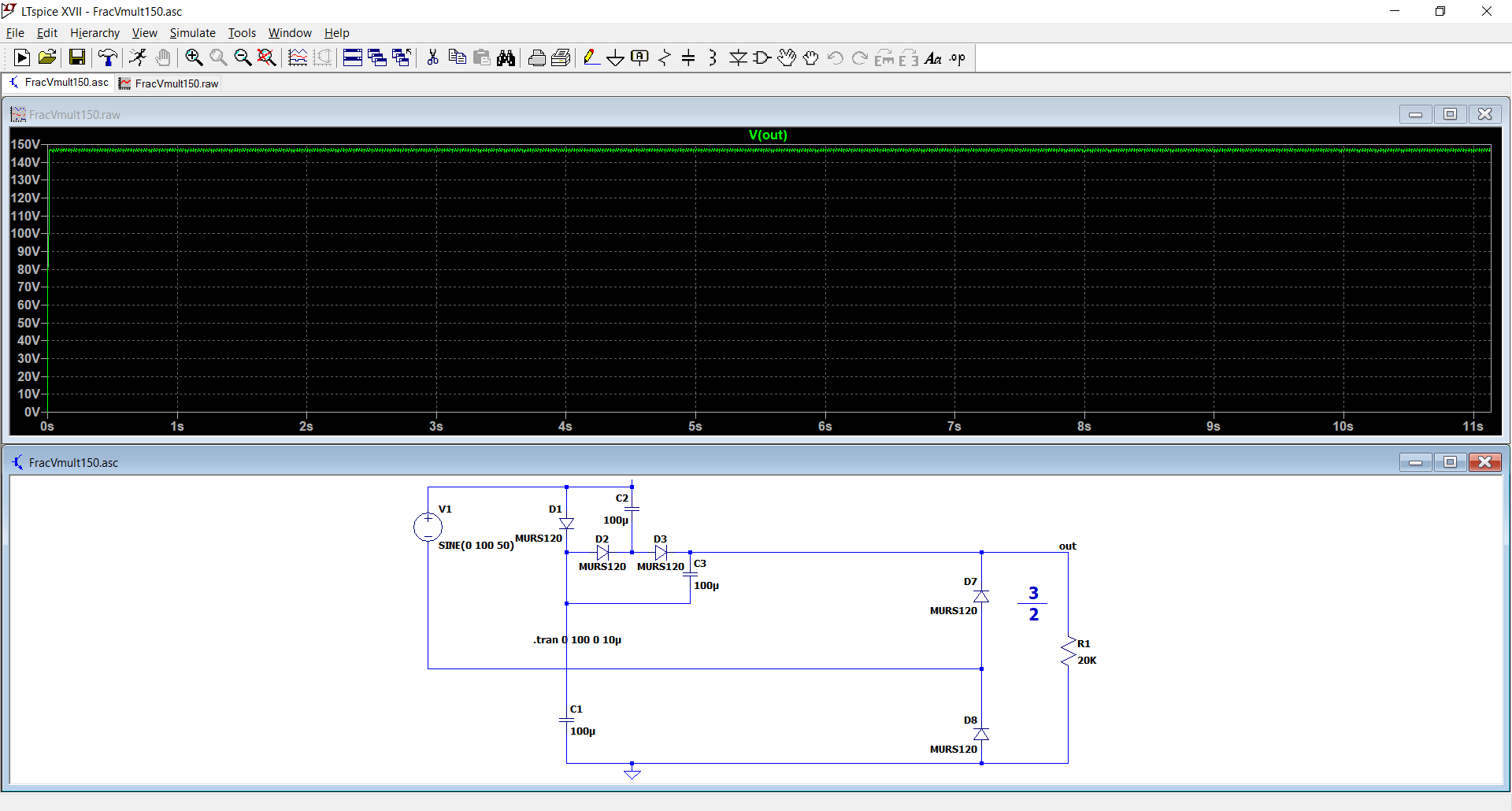
Here are some more examples.
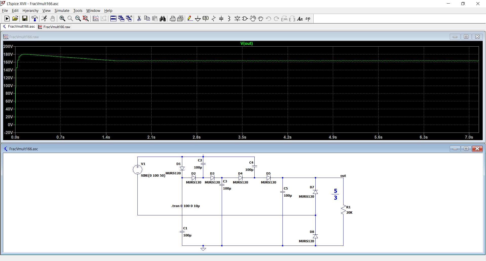
First, the 5/3 (1.666x) one:
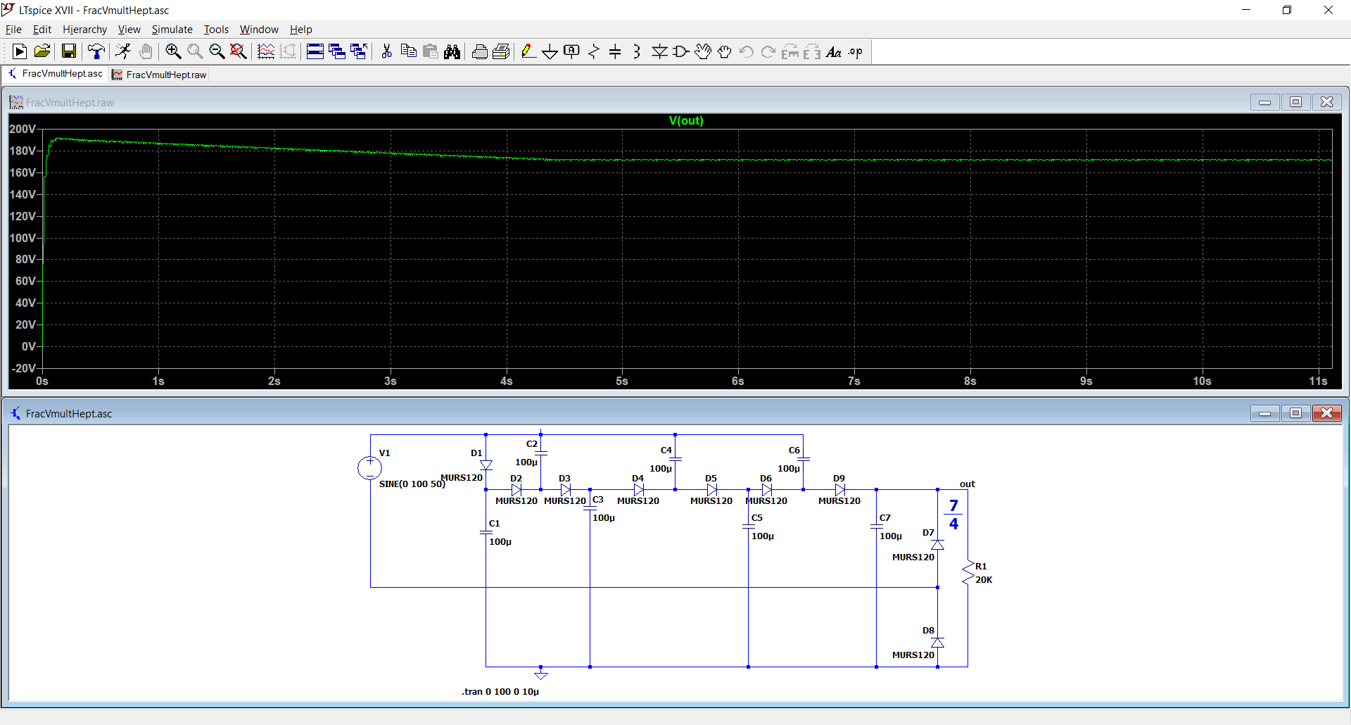
Then, the 7/4 (1.75x):
Many other values are possible using the same principles. Nowadays however, the usefulness of these circuits is reduced: to squeeze the last % of possible efficiency out of a supply, the rectifiers use controlled switches anyway: active bridges, etc., and they allow any fantasy when driven suitably.
For DIYers, these circuits make sense: they are not obsessed by efficiency, and the scheme allows the use of transformers that would be useless otherwise.
For industrial, EHV circuits, they could be useful too: at voltages >>10kV, stacking is necessary, and the need to add a drive circuit to control the switch adds to the complications. Diodes are two-terminal devices, and they can be connected in series without great difficulties.
So, the fractional nut has been cracked open, but what about stepdown?
Unfortunately, that one is still intact, and I have reasons to think that it might be uncrackable with devices using only natural switching: the switching sequence always requires an "unnatural" conduction, requiring a smarter switch, but who knows.....
The front of "traditional" voltage multipliers has been extremely quiet for years, decades, and even a whole century: all of the major topologies like Greinacher, Schenkel, Latour, Delon, Villard, Cockcroft, Dickson, etc. have been invented ~100 years ago or more. There have been minor topology changes for some, like a different connection of capacitors, but the base structure remained the same.
By "traditional", I mean those based on autonomous switching elements, ie. diodes, capable of deciding by themselves when to conduct and when to block, based on the polarity they see.
The arrival of practical controlled switches in the seventies revolutionized the field, allowing charge pumps to work as step-down or fractional converters.
However, there is a tacit, implicit comprehension that traditional multipliers are unable to perform such acrobatics, and that they are limited to a multiplication by n, with n being any integer, thereby ruling out fractional multipliers and step-down converters since the only integer value <1 is 0, which is possible of course, but not extra-useful in practice.
Tentatives have been made with quirky circuits that appear to work as fractional converters under very special conditions, but in practice they are just topologies having high, concentrated losses for their theoretical voltage, regressing to a lower order multiplication ratio as soon as they see a significant load. This means a high internal resistance, heavy losses and heavy stresses on one or two components.
In short, they are a cheat, and don't really qualify.
Thus, there seems to be no hope, and the traditional view seems to hold, even though there is no actual demonstration that a fractional multiplier is impossible.
Is it really the case?
No.
And here is the proof:
It is a working example of 4/3rd multiplier (I can see some of you frantically typing, trying to find a precedent, but I don't think it will return a hit).
At first sight, exchanging fractional charge quantities using just "dumb", autonomous switching devices seems impossible, but a workaround is possible: if you connect the inputs of two different multipliers in series, and their outputs in parallel, they will have to split the charge and find an equilibrium satisfying the input and output voltage conditions for both.
In this example, the upper multiplier is a doubler, and the lower one a quadrupler.
Let's call the input of the upper one V1, and the lower one V2.
We can write: 2*V1=Vout and 4*V2=Vout, and also V1+V2=Vin
We can sum twice the first equation to the second: 4*(V1+V2)=3*Vout. As V1+V2= Vin, 4*Vin=3*Vout, thus Vout=4*Vin/3.
Other factors are possible; in fact, the number is ~limitless, but in practice very complicated ratio's are not very advantageous, because they require lots of components.
The 3/2 ratio is particularly interesting: it has a reasonable parts count, and sits just between a plain rectifier and a doubler. Many DIYers have been confronted to the situation where a transformer delivers a voltage just too low with a simple rectifier, but much too high with a doubler. The 3/2 option is a neat tradeoff in this case.
Here are some more examples.
First, the 5/3 (1.666x) one:
Then, the 7/4 (1.75x):
Many other values are possible using the same principles. Nowadays however, the usefulness of these circuits is reduced: to squeeze the last % of possible efficiency out of a supply, the rectifiers use controlled switches anyway: active bridges, etc., and they allow any fantasy when driven suitably.
For DIYers, these circuits make sense: they are not obsessed by efficiency, and the scheme allows the use of transformers that would be useless otherwise.
For industrial, EHV circuits, they could be useful too: at voltages >>10kV, stacking is necessary, and the need to add a drive circuit to control the switch adds to the complications. Diodes are two-terminal devices, and they can be connected in series without great difficulties.
So, the fractional nut has been cracked open, but what about stepdown?
Unfortunately, that one is still intact, and I have reasons to think that it might be uncrackable with devices using only natural switching: the switching sequence always requires an "unnatural" conduction, requiring a smarter switch, but who knows.....
Attachments
Stochastic RMS to DC converters
The subject of RMS to DC conversion has already been thoroughly explored, resulting in tens (if not hundreds) of methods/topologies/patents.
Does an unturned stone remain?
Maybe.
This is a possible example:
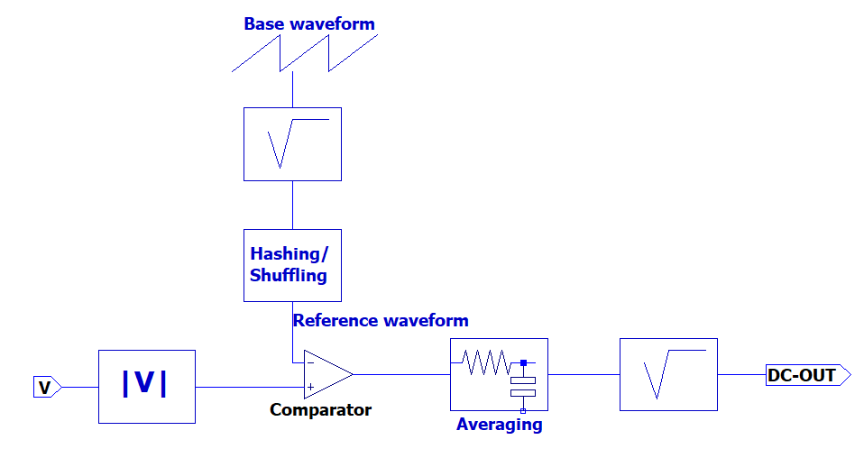
A reference waveform is compared to the input signal, preferably passed through a precision rectifier, AKA absolute value circuit.
The reference waveform is a processed √t starting like that:
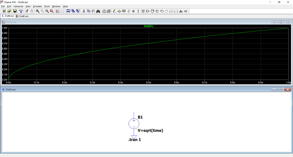
If you compare any waveform to this modified sawtooth, the averaged result will always be the mean square value. This is valid for any waveform or any frequency: the incident signal can have a much higher or a much lower frequency than the reference, it doesn't matter provided the averaging time is long enough. You have to take my word for it: if you wanted a formal proof, you are ~40 years too late. Nowadays, I don't bother writing equations, I just rely on my sixth sense (AKA gut feeling): I simply know it is true. For a steady DC voltage, it is trivial, for other signals it is less obvious, precisely because it is a stochastic process: if you try to decompose the resulting squarewave into individual bits, none of them makes sense in isolation. Only an average taken on a sufficient number of samples will converge towards the desired value.
Once you have the mean square, you just need to take the square root to arrive at the RMS value.
This simplified scheme has an issue though: if the waveforms frequencies or their multiples/submultiples are close, beat effects due to aliasing will appear, making the end result fluctuate, or even stay stuck at a wrong value in case of synchronism with an unfavourable phase.
That is the reason for the hashing/shuffling function block: you cut the initial waveform into a large number (1024 for example) of small pieces, and you rearrange them in a different, random order. The next cycle, you do the same using another sequence, etc etc.
With 1024 samples, you must have something like 1024! sequences possible, which should be sufficient to last for a century or two.
The result will look like white noise, except the amplitudes distribution will be skewed, and remain the same as the original waveform, meaning the conversion process will work in exactly the same way.
The difference is that with a random, noise-like waveform, no coherence is possible, and all the aliasing effects are eliminated.
Note that the block-diagram above is mostly explanatory: the real implementation would be somewhat different.
Firstly the reference signal generator would be digital, a µC or FPGA with a D/A convertor.
Secondly, the final √ function would be implicit rather than explicit, like in many similar converters: it simplifies the circuit and improves the dynamic range.
And finally there would be no absolute value generator: a big advantage of this scheme is the combination of extreme speed (sub-ns comparators are no problem) and fine accuracy: a good comparator can resolve much less than 1 mV.
A conventional absolute value circuit would have trouble keeping up with such performances, and would ruin the ability to process accurately small amplitude, high frequency signals.
The best method would be the duplication of the circuit: one for the positive, and its complement for the negative. They would then be combined in a digital gate before being averaged.
This method has the potential to match the best present ones regarding dynamic range and resolution, but at speeds close to RF.
That said, aliasing is not that much of a problem: I have used a parent scheme in my HP428 clone, but heavily simplified.
This is the internal schematic of the blanked box of the schematic:
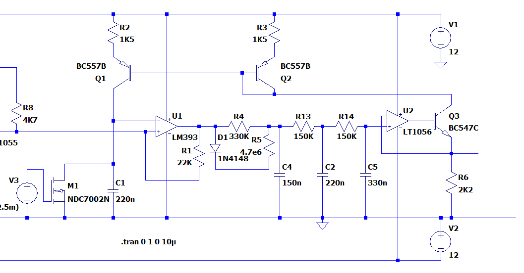
In this circuit, there is no hashing or randomizing of the reference waveform: it is just the raw, fixed-frequency sawtooth. The squaring process is also heavily simplified: it is performed by the comparator U1, with the input signal both PWM modulated and sent to the OC output via R1. The diode and R5 correct the asymmetry of the output impedance before driving the averaging network.
The final square-root function is performed implicitly, thanks to a feedback from the output controlling the charge current of C1. This acts as a linear AGC, resulting in an implicit square-root extraction.
The operation frequency is 400Hz, set by the sawtooth reset pulse via M1.
The circuit is minimally simplistic and has no protection against aliasing, but in practice it is never noticeable, unless you are really determined to cause it (I carefully tested this aspect before including it in the final build).
The subject of RMS to DC conversion has already been thoroughly explored, resulting in tens (if not hundreds) of methods/topologies/patents.
Does an unturned stone remain?
Maybe.
This is a possible example:
A reference waveform is compared to the input signal, preferably passed through a precision rectifier, AKA absolute value circuit.
The reference waveform is a processed √t starting like that:
If you compare any waveform to this modified sawtooth, the averaged result will always be the mean square value. This is valid for any waveform or any frequency: the incident signal can have a much higher or a much lower frequency than the reference, it doesn't matter provided the averaging time is long enough. You have to take my word for it: if you wanted a formal proof, you are ~40 years too late. Nowadays, I don't bother writing equations, I just rely on my sixth sense (AKA gut feeling): I simply know it is true. For a steady DC voltage, it is trivial, for other signals it is less obvious, precisely because it is a stochastic process: if you try to decompose the resulting squarewave into individual bits, none of them makes sense in isolation. Only an average taken on a sufficient number of samples will converge towards the desired value.
Once you have the mean square, you just need to take the square root to arrive at the RMS value.
This simplified scheme has an issue though: if the waveforms frequencies or their multiples/submultiples are close, beat effects due to aliasing will appear, making the end result fluctuate, or even stay stuck at a wrong value in case of synchronism with an unfavourable phase.
That is the reason for the hashing/shuffling function block: you cut the initial waveform into a large number (1024 for example) of small pieces, and you rearrange them in a different, random order. The next cycle, you do the same using another sequence, etc etc.
With 1024 samples, you must have something like 1024! sequences possible, which should be sufficient to last for a century or two.
The result will look like white noise, except the amplitudes distribution will be skewed, and remain the same as the original waveform, meaning the conversion process will work in exactly the same way.
The difference is that with a random, noise-like waveform, no coherence is possible, and all the aliasing effects are eliminated.
Note that the block-diagram above is mostly explanatory: the real implementation would be somewhat different.
Firstly the reference signal generator would be digital, a µC or FPGA with a D/A convertor.
Secondly, the final √ function would be implicit rather than explicit, like in many similar converters: it simplifies the circuit and improves the dynamic range.
And finally there would be no absolute value generator: a big advantage of this scheme is the combination of extreme speed (sub-ns comparators are no problem) and fine accuracy: a good comparator can resolve much less than 1 mV.
A conventional absolute value circuit would have trouble keeping up with such performances, and would ruin the ability to process accurately small amplitude, high frequency signals.
The best method would be the duplication of the circuit: one for the positive, and its complement for the negative. They would then be combined in a digital gate before being averaged.
This method has the potential to match the best present ones regarding dynamic range and resolution, but at speeds close to RF.
That said, aliasing is not that much of a problem: I have used a parent scheme in my HP428 clone, but heavily simplified.
This is the internal schematic of the blanked box of the schematic:
In this circuit, there is no hashing or randomizing of the reference waveform: it is just the raw, fixed-frequency sawtooth. The squaring process is also heavily simplified: it is performed by the comparator U1, with the input signal both PWM modulated and sent to the OC output via R1. The diode and R5 correct the asymmetry of the output impedance before driving the averaging network.
The final square-root function is performed implicitly, thanks to a feedback from the output controlling the charge current of C1. This acts as a linear AGC, resulting in an implicit square-root extraction.
The operation frequency is 400Hz, set by the sawtooth reset pulse via M1.
The circuit is minimally simplistic and has no protection against aliasing, but in practice it is never noticeable, unless you are really determined to cause it (I carefully tested this aspect before including it in the final build).
Attachments
You are welcome.
A transformer-less AC voltage doubler
Here is a lighter, but possibly useful idea.
It is a voltage multiplier, but it operates fully in AC, input and output. It can convert a 115V mains into a 230V output, and could be of some use to DIYers on the other side of the pond: when you want to convert an exclusively European equipment to the US mains, you have the choice between changing the internal transformer (or supply) or using an autoformer, none of which is very appealing: no one likes the idea of butchering an equipment or adding a bulky, heavy piece of kit to the existing setup.
This converter is purely electronic, takes little room or power, and could generally be tucked inside the equipment to convert, without any visible exterior sign.
It is far from perfect: the frequency will remain 60Hz, not 50, and the waveform is not sinusoidal, but it isn't too aggressive either.
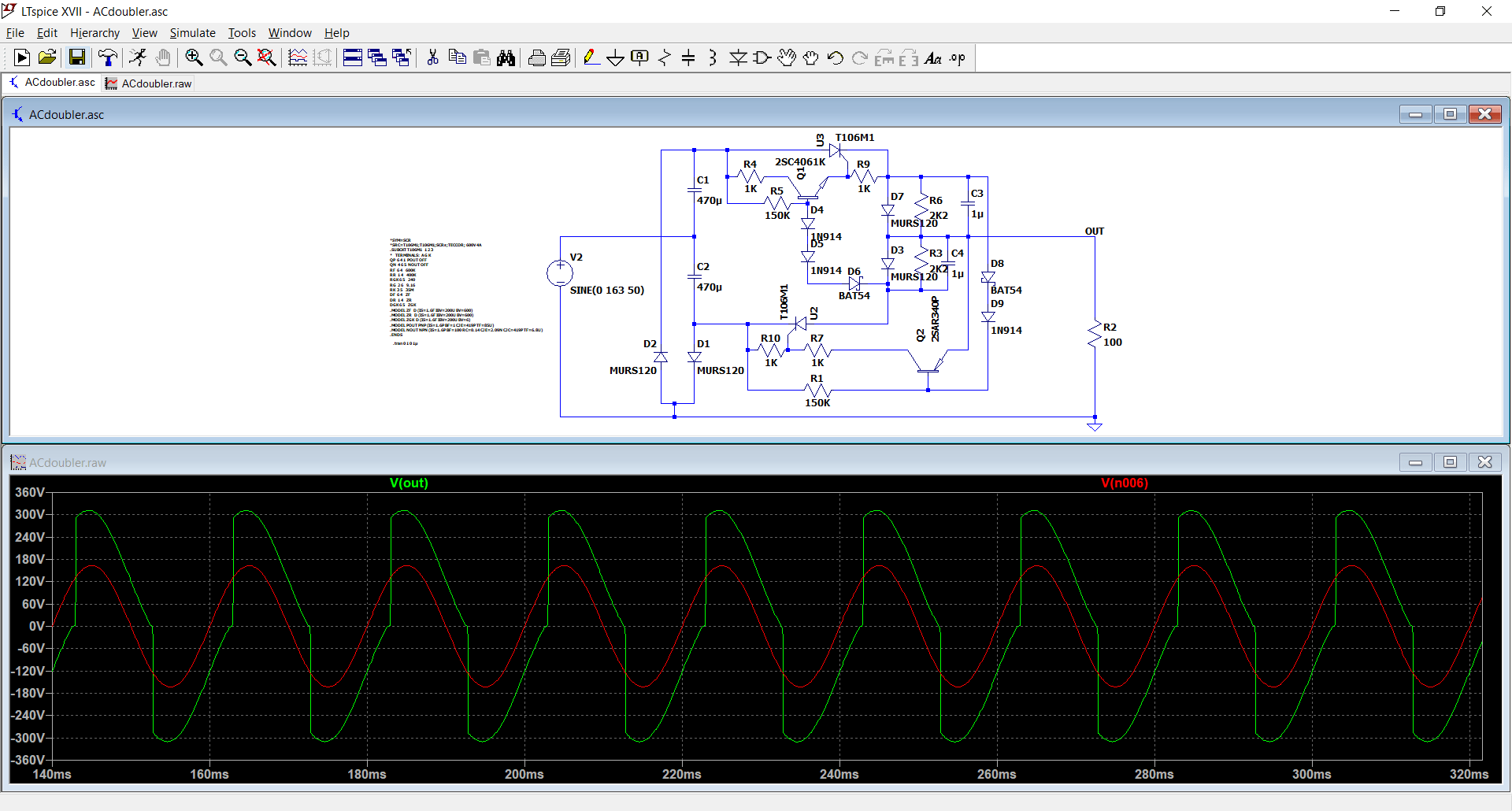
In practice, the transistors can be MPSA42/92, I used these types for simulation convenience
A transformer-less AC voltage doubler
Here is a lighter, but possibly useful idea.
It is a voltage multiplier, but it operates fully in AC, input and output. It can convert a 115V mains into a 230V output, and could be of some use to DIYers on the other side of the pond: when you want to convert an exclusively European equipment to the US mains, you have the choice between changing the internal transformer (or supply) or using an autoformer, none of which is very appealing: no one likes the idea of butchering an equipment or adding a bulky, heavy piece of kit to the existing setup.
This converter is purely electronic, takes little room or power, and could generally be tucked inside the equipment to convert, without any visible exterior sign.
It is far from perfect: the frequency will remain 60Hz, not 50, and the waveform is not sinusoidal, but it isn't too aggressive either.
In practice, the transistors can be MPSA42/92, I used these types for simulation convenience
Attachments
I think that your fractional voltage multipliers would be very useful for those of us building tube amplifier supplies with off the shelf power transformers. I 'm already thinking of a power transformer I have that has never found use because of it's 'inconvenient' winding ratio.
More immediately, I have been working on a circuit (for a couple of years now) that in the breadboard has been using transformers outputting higher voltage than needed into a dc filament supply rectifier. Presently, the combined total of power being wasted across the four supplies required for two channels is 20Watts. I have been scouting for affordable transformers to provide the right voltages but your posts make me wonder if there might be a path to 'Fractional Reduction' with the existing transformers (as they are).
More immediately, I have been working on a circuit (for a couple of years now) that in the breadboard has been using transformers outputting higher voltage than needed into a dc filament supply rectifier. Presently, the combined total of power being wasted across the four supplies required for two channels is 20Watts. I have been scouting for affordable transformers to provide the right voltages but your posts make me wonder if there might be a path to 'Fractional Reduction' with the existing transformers (as they are).
AC voltage halvers
For the sake of completeness (purely), here are the "dual" equivalents of the previous one.
They change a 230V input into a 115V output, and they don't rely on a transformer, of course. In their present form, they are purely conceptual: they have never been tested or used, not even breadboarded.
They certainly have issues: for example the startup/inrush behaviour, but if someone needs such a function, they are a good starting point/initial framework to start with.
Here is the first, simpler version:
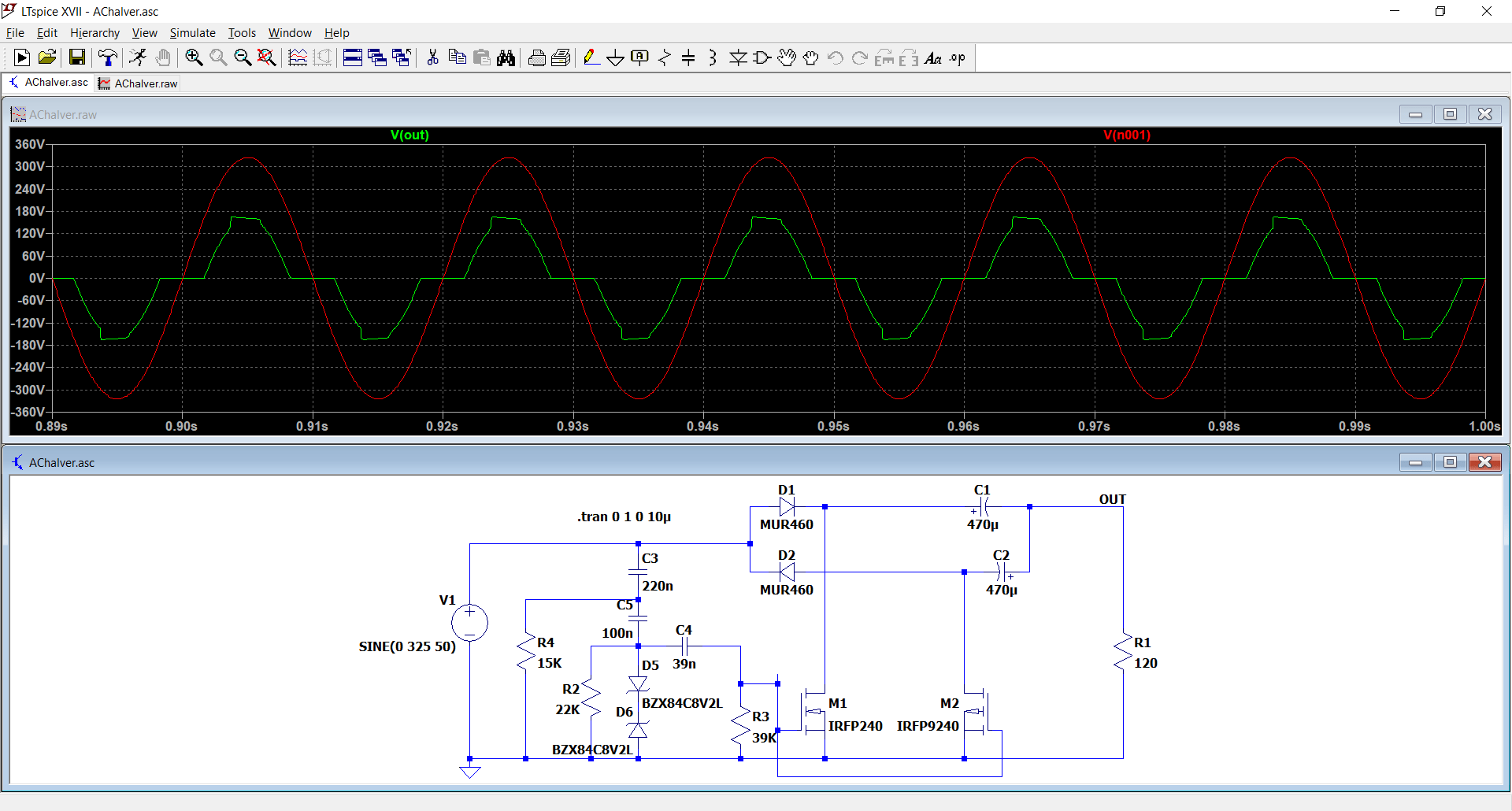
Its problem is the use of a power, high-voltage PMOS, which are very rare beasts. They need to withstand the full peak input voltage, plus some margin, at least 400V, preferably 500V or 600V.
The sim cheats with a 200V IRF9240.
This variant is more complex, but it only uses more common N-types:
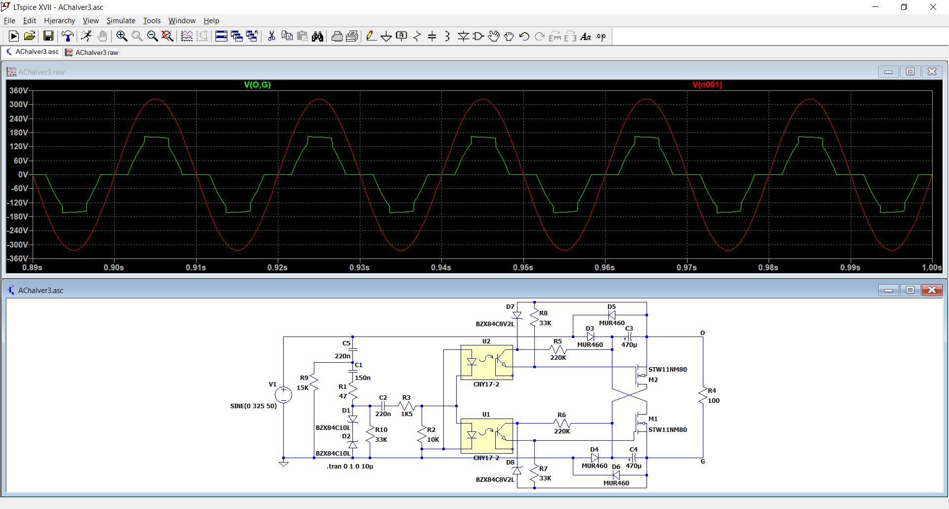
Both are based on the same principle: a constant voltage is subtracted from each sine arch. The voltage is stored in capacitors, and the complicated part of the scheme is the removal of the excess charge of the capacitors after they have been used in the forward path.
The charge is dumped into the load during the opposite part of the cycle, at around 90° and 270°, which explains the little "hat" on the top of the waveforms. This also guarantees an exact halving of the input voltage
The waveform is therefore far from a sinewave, but the peak voltage is correct, which matters for capacitively filtered supplies. The average voltage is too low, but it is rather good news for inductive components, and the rms voltage is too low too, meaning that loads using power, like heaters will receive 10% less voltage.
Both suffer from a high inrush current. It can be eliminated by including series diodes in the drains of MOS, but at startup this will cause the load to see the full input voltage. Thus, an unfinished work
For the sake of completeness (purely), here are the "dual" equivalents of the previous one.
They change a 230V input into a 115V output, and they don't rely on a transformer, of course. In their present form, they are purely conceptual: they have never been tested or used, not even breadboarded.
They certainly have issues: for example the startup/inrush behaviour, but if someone needs such a function, they are a good starting point/initial framework to start with.
Here is the first, simpler version:
Its problem is the use of a power, high-voltage PMOS, which are very rare beasts. They need to withstand the full peak input voltage, plus some margin, at least 400V, preferably 500V or 600V.
The sim cheats with a 200V IRF9240.
This variant is more complex, but it only uses more common N-types:
Both are based on the same principle: a constant voltage is subtracted from each sine arch. The voltage is stored in capacitors, and the complicated part of the scheme is the removal of the excess charge of the capacitors after they have been used in the forward path.
The charge is dumped into the load during the opposite part of the cycle, at around 90° and 270°, which explains the little "hat" on the top of the waveforms. This also guarantees an exact halving of the input voltage
The waveform is therefore far from a sinewave, but the peak voltage is correct, which matters for capacitively filtered supplies. The average voltage is too low, but it is rather good news for inductive components, and the rms voltage is too low too, meaning that loads using power, like heaters will receive 10% less voltage.
Both suffer from a high inrush current. It can be eliminated by including series diodes in the drains of MOS, but at startup this will cause the load to see the full input voltage. Thus, an unfinished work
Attachments
Tandem regulators
Series and shunt regulators can be associated in order to improve some performances. They are generally known as two-quadrant regulators, and the main goal is usually the improvement of dynamic performances: a classical series regulator, having to deliver an output anywhere between 0 and Imax demands difficult tradeoffs regarding the compensation.
It has to remain stable and well-behaved, despite the huge variation of the ballast's transconductance induced by the current change, and it has to deal with many types of loads, including purely capacitive ones.
To eliminate the overshoot after the trailing edge of a current step and to keep the output impedance ~constant over a wide range of currents, a two-quadrant output is an effective solution.
One of the simplest example of such a regulator is a class AB push-pull stage.
It is possible to go much further in the association, and establish a strong link between the series and shunt parts, to make them operate in synergy.
With a properly implemented synergy, the end result becomes much greater than the mere sum of its parts: this becomes a "tandem" regulator, a term I coined myself and which seems appropriate.
Note that tandem regulators are a subset of two-quadrant regulators, but not all 2Q's are tandem: in a class AB stage for example, the link between the two is absolutely minimalistic, passive and "dumb", consisting of a diode string or a transistor base-spreader. In a tandem regulator, the two halves actively communicate, and influence one another.
I have tried to introduce the concept earlier but it was not received enthusiastically, to use an euphemism:
https://www.diyaudio.com/community/threads/tandem-regulators.265435/post-4134147
As the reactions to the concept were scepticism and criticism, I concluded that continuing to post my findings was a waste of time, yet I continue to think that the concept is not worthless.
Here is another tentative.
The simplest form of a tandem regulator would be this:
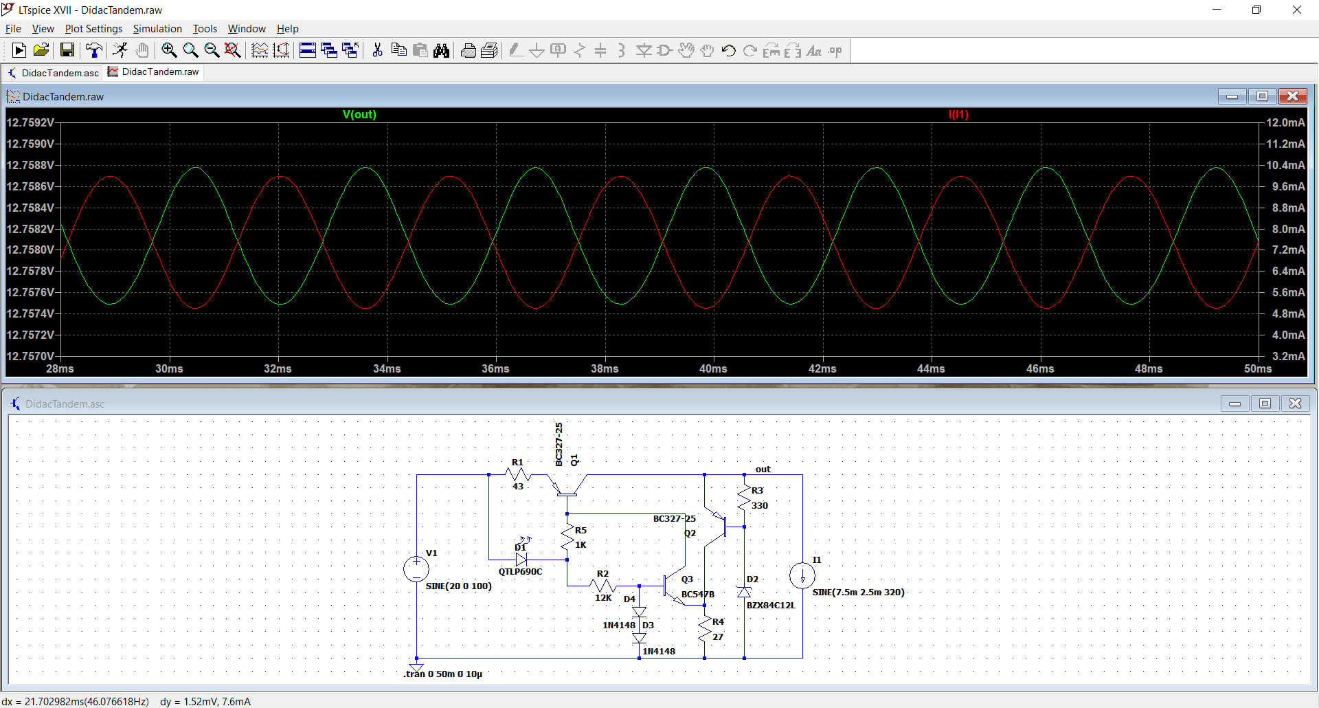
Q1 is the series part, Q2 is a classical amplified-zener shunt, and Q3 makes the link.
It does work, of course, but it is possible to do better:
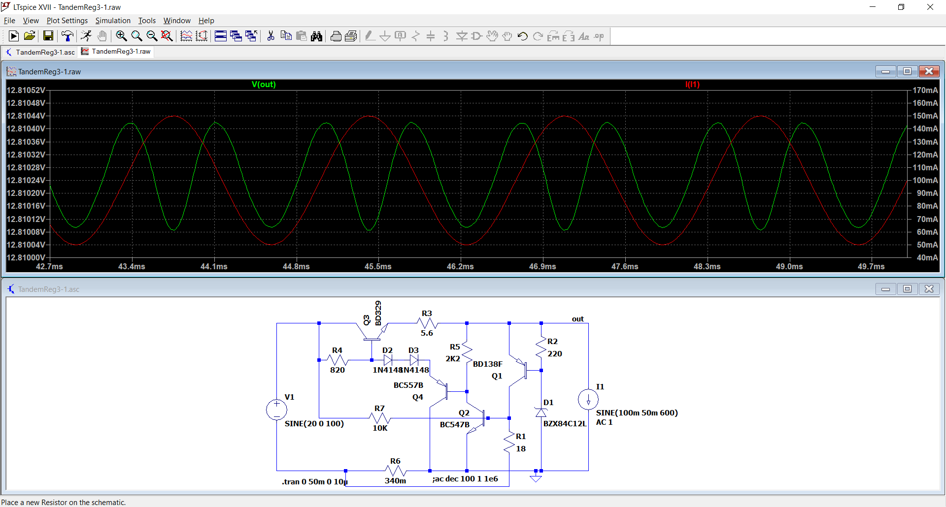
This one has more amplification, and includes compensation resistors (since the compensation is optimal, the output residue has twice the frequency of the stimulus current).
Let's go a step further, and include an active compensation:

The sim illustrates clearly the two-quadrant capability. Here, the reference voltage is provided by V2, and this voltage is reproduced exactly at the output.
The circuit uses a mix of negative and positive feedback to arrive at excellent performances (the output impedance is well under 1 milliohm).
The high input impedance seen from the reference input, the extreme fidelity of the output to the input and the deterministically controlled quiescent (shunt) current combined with the two quadrant capability opens intriguing possibilities: the circuit can also operate as a high-performance, power buffer, or a near-ideal output stage.
This sim shows the circuit in this role, with only minimal adaptations. The level is kept to a reasonable 4V pp, because it is a medium power supply, not suited to a full amplitude swing into 4 ohm:
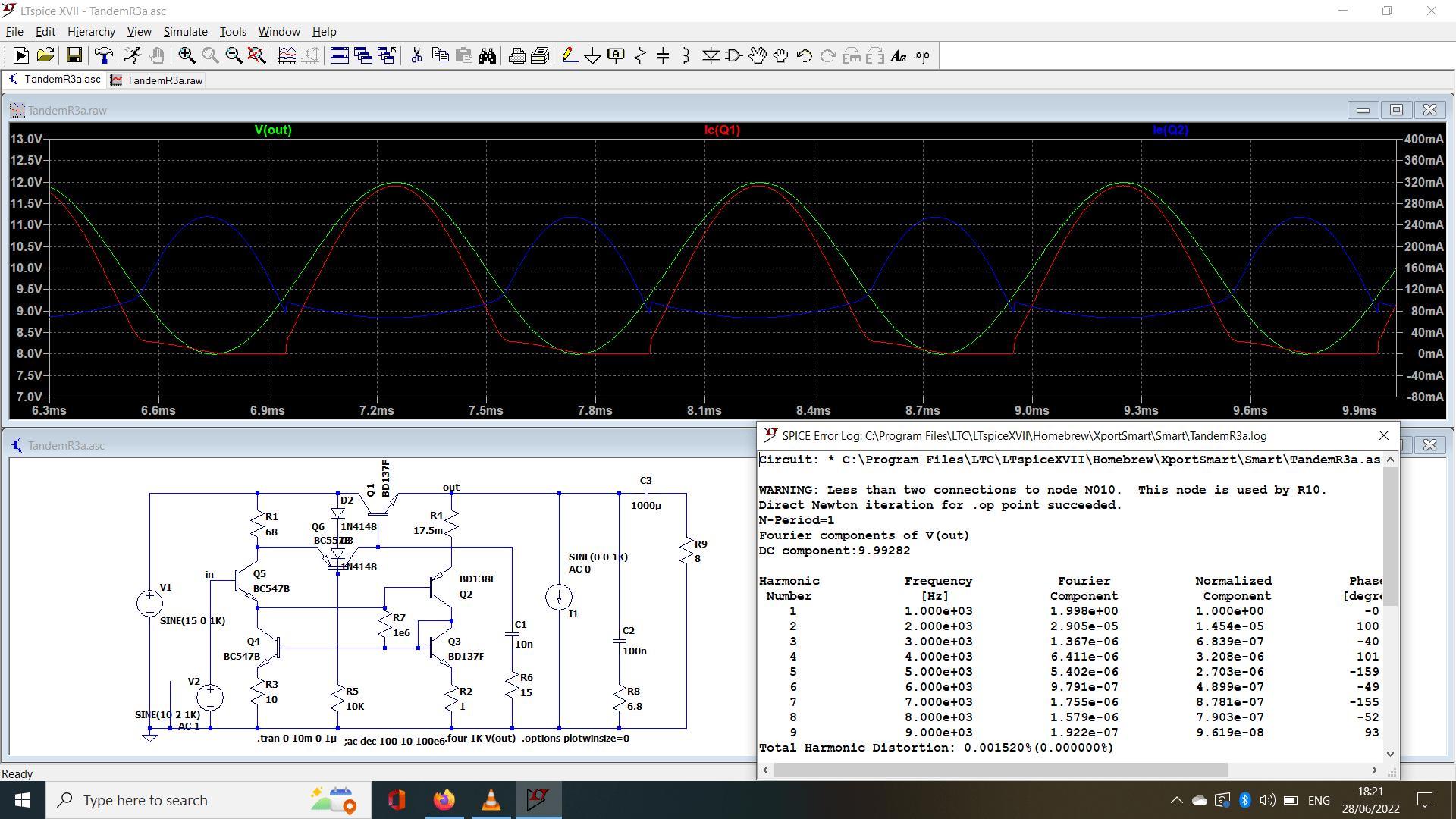
The simulated THD is ~15ppm, in reality it would probably be 2 or 3 times higher, but it would remain excellent for a naked OP stage. The circuit is half non-switching: one half (the shunt part) always conducts.
The small-signal BW is nice too, meaning the integration of this stage in a GNFB loop would pose no problem:
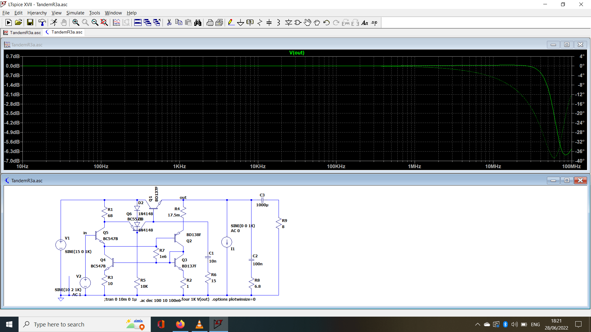
It easily reaches 30MHz, using only common, GP transistors.
This is all very nice, but that's theory and sim. What about the reality?
I made some tests, and the reality agrees with the sims -up to a point-: as soon as you draw current, there is a differential heating of the transistors, and this degrades the ideal static compensations.
The effect is not caused by Vbe changes, because the circuit is mostly immune to them, but by kT/q and parasitic resistances variations: metallizations, bonding wires, etc.
Thus, ppm performance is not realistic in the real world, but the performances remain outstanding.
The circuit is somewhat quirky: for the audio range, the input impedance is ~200K, but with a minus sign in front of it.... Somewhat disconcerting, but not really a problem: by paralleling a 180K, the impedance will become some megohms, and turn positive. At higher frequencies, a RC circuit is required to keep the impedance positive.
These are minor issues if you are aware of them.
This shows that this class of regulators are capable of unusual tricks, in addition to their superb performance as ordinary regulators.
Note that the tandem principle can be implemented using a variety of other topologies
Series and shunt regulators can be associated in order to improve some performances. They are generally known as two-quadrant regulators, and the main goal is usually the improvement of dynamic performances: a classical series regulator, having to deliver an output anywhere between 0 and Imax demands difficult tradeoffs regarding the compensation.
It has to remain stable and well-behaved, despite the huge variation of the ballast's transconductance induced by the current change, and it has to deal with many types of loads, including purely capacitive ones.
To eliminate the overshoot after the trailing edge of a current step and to keep the output impedance ~constant over a wide range of currents, a two-quadrant output is an effective solution.
One of the simplest example of such a regulator is a class AB push-pull stage.
It is possible to go much further in the association, and establish a strong link between the series and shunt parts, to make them operate in synergy.
With a properly implemented synergy, the end result becomes much greater than the mere sum of its parts: this becomes a "tandem" regulator, a term I coined myself and which seems appropriate.
Note that tandem regulators are a subset of two-quadrant regulators, but not all 2Q's are tandem: in a class AB stage for example, the link between the two is absolutely minimalistic, passive and "dumb", consisting of a diode string or a transistor base-spreader. In a tandem regulator, the two halves actively communicate, and influence one another.
I have tried to introduce the concept earlier but it was not received enthusiastically, to use an euphemism:
https://www.diyaudio.com/community/threads/tandem-regulators.265435/post-4134147
As the reactions to the concept were scepticism and criticism, I concluded that continuing to post my findings was a waste of time, yet I continue to think that the concept is not worthless.
Here is another tentative.
The simplest form of a tandem regulator would be this:
Q1 is the series part, Q2 is a classical amplified-zener shunt, and Q3 makes the link.
It does work, of course, but it is possible to do better:
This one has more amplification, and includes compensation resistors (since the compensation is optimal, the output residue has twice the frequency of the stimulus current).
Let's go a step further, and include an active compensation:
The sim illustrates clearly the two-quadrant capability. Here, the reference voltage is provided by V2, and this voltage is reproduced exactly at the output.
The circuit uses a mix of negative and positive feedback to arrive at excellent performances (the output impedance is well under 1 milliohm).
The high input impedance seen from the reference input, the extreme fidelity of the output to the input and the deterministically controlled quiescent (shunt) current combined with the two quadrant capability opens intriguing possibilities: the circuit can also operate as a high-performance, power buffer, or a near-ideal output stage.
This sim shows the circuit in this role, with only minimal adaptations. The level is kept to a reasonable 4V pp, because it is a medium power supply, not suited to a full amplitude swing into 4 ohm:
The simulated THD is ~15ppm, in reality it would probably be 2 or 3 times higher, but it would remain excellent for a naked OP stage. The circuit is half non-switching: one half (the shunt part) always conducts.
The small-signal BW is nice too, meaning the integration of this stage in a GNFB loop would pose no problem:
It easily reaches 30MHz, using only common, GP transistors.
This is all very nice, but that's theory and sim. What about the reality?
I made some tests, and the reality agrees with the sims -up to a point-: as soon as you draw current, there is a differential heating of the transistors, and this degrades the ideal static compensations.
The effect is not caused by Vbe changes, because the circuit is mostly immune to them, but by kT/q and parasitic resistances variations: metallizations, bonding wires, etc.
Thus, ppm performance is not realistic in the real world, but the performances remain outstanding.
The circuit is somewhat quirky: for the audio range, the input impedance is ~200K, but with a minus sign in front of it.... Somewhat disconcerting, but not really a problem: by paralleling a 180K, the impedance will become some megohms, and turn positive. At higher frequencies, a RC circuit is required to keep the impedance positive.
These are minor issues if you are aware of them.
This shows that this class of regulators are capable of unusual tricks, in addition to their superb performance as ordinary regulators.
Note that the tandem principle can be implemented using a variety of other topologies
Attachments
small question from a noob, enjoying your attic legacy:
will a (your) tandem regulator source and sink current to mantain the desired voltage?
will a (your) tandem regulator source and sink current to mantain the desired voltage?
Yes Sir, in this pic, you see that the load is a purely AC current source, swinging from +100mA to -100mA, with no static load or offset current in sight:
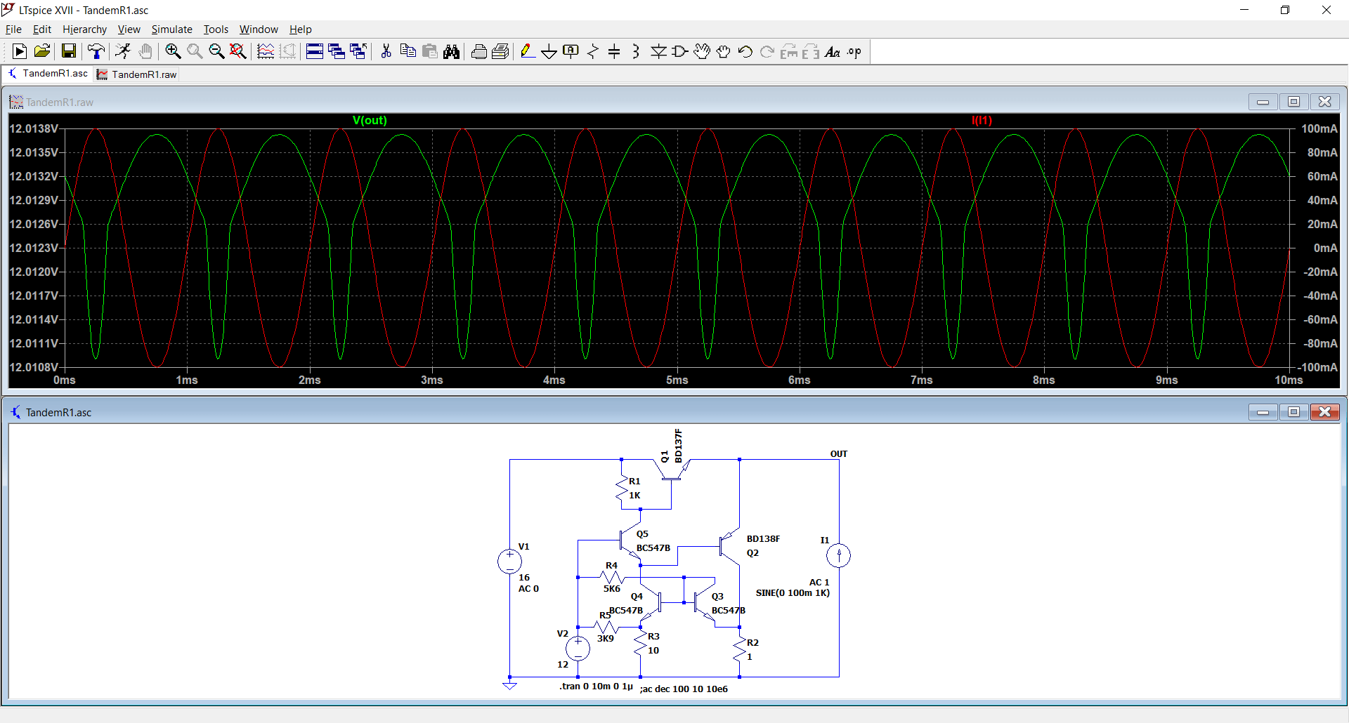
You see that the response is different for negative and positive excursions; this explains the fact that the THD is mainly composed of second/even harmonics.
It is certainly an aspect that could be improved/equalized in case it matters, but I didn't focus on such things: this is just a high-level introduction to the various concepts, not complete projects.
If you want to use the concepts, you need to make your own homework and personalize them according to your needs. That said, if you look at the vertical scale on the left, you can see that in absolute terms, the difference is not that huge
Full-wave current doubler
Here is another little circuit that tube-lovers might find useful: it is a FW current doubler (and thus voltage halver), but with an interesting feature.
Usually, current doublers use the positive half-cycle to charge two capacitors in series, and the negative one to connect them in parallel, meaning they are half-wave. Another similar circuit is required, together with an inverting circuit to be able to use the whole cycle actively.
This doubler works as a half-wave doubler, with a single controlled switch (a MOSFET), but it operates on an already rectified full-wave input: the charging phase takes place during the peaks of the waveform, and the parallel discharge during the troughs, thanks to a peculiar control of the MOS.
As an added benefit, the final ripple frequency is 4*Fmains, thus 200Hz with a 50Hz mains, which eases the filtering:
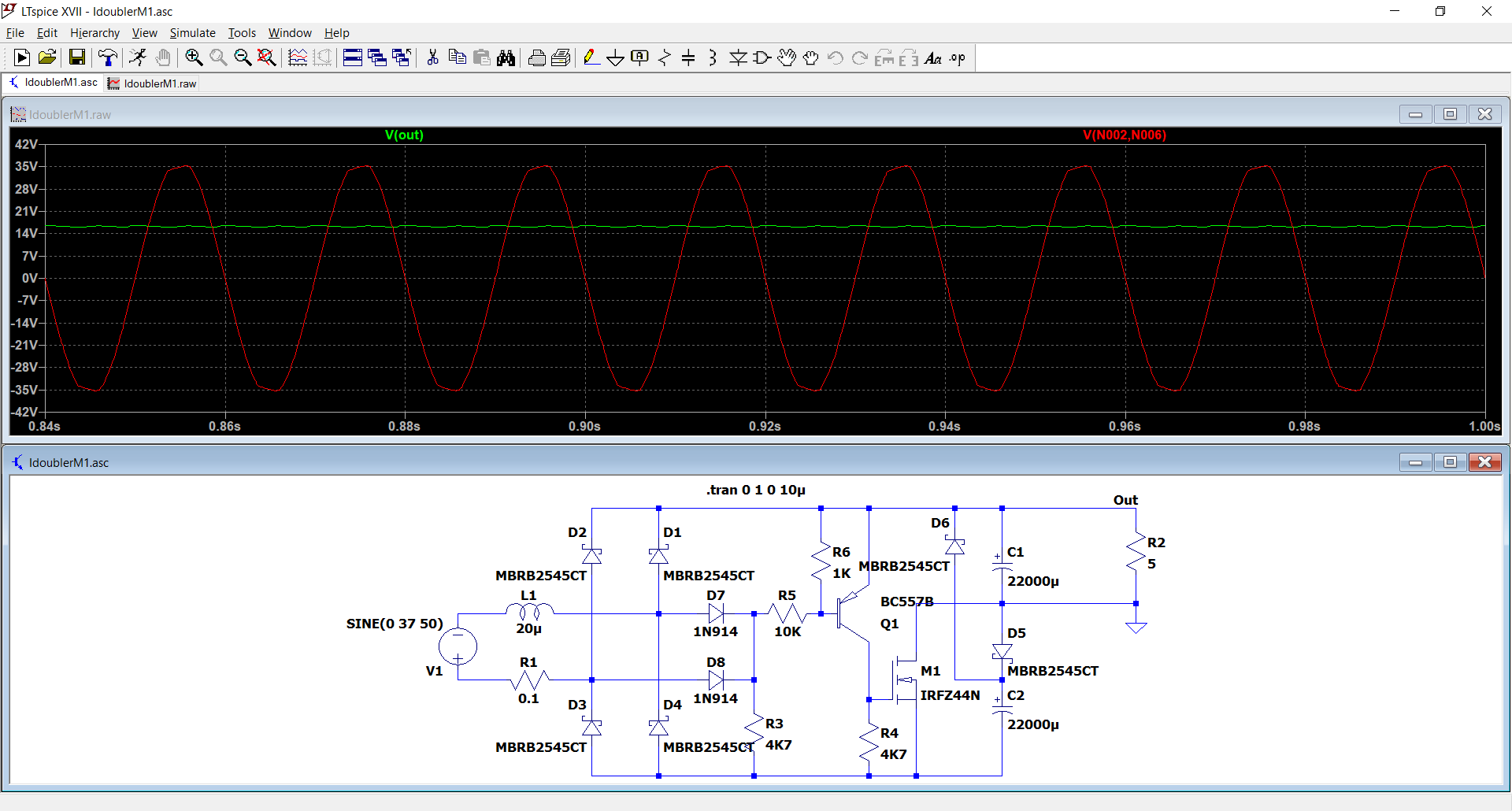
It has a number of potential applications, but one that comes to mind is as a DC heater supply, possibly with a transformer having the wrong voltage, or when there is a mix of 6V and 12V tubes: you simply need to add an isolation diode to the FW rectified output, to isolate it from the 12V filtering capacitor.
The same principle could be used to create half-voltage rails, in an amplifier for example: the +/-50V would go to the power amplifier, and the +/-25V would be used for the lower power circuits, without requiring an additional transformer or winding, or wasting too much power in a regulator.
Here is another little circuit that tube-lovers might find useful: it is a FW current doubler (and thus voltage halver), but with an interesting feature.
Usually, current doublers use the positive half-cycle to charge two capacitors in series, and the negative one to connect them in parallel, meaning they are half-wave. Another similar circuit is required, together with an inverting circuit to be able to use the whole cycle actively.
This doubler works as a half-wave doubler, with a single controlled switch (a MOSFET), but it operates on an already rectified full-wave input: the charging phase takes place during the peaks of the waveform, and the parallel discharge during the troughs, thanks to a peculiar control of the MOS.
As an added benefit, the final ripple frequency is 4*Fmains, thus 200Hz with a 50Hz mains, which eases the filtering:
It has a number of potential applications, but one that comes to mind is as a DC heater supply, possibly with a transformer having the wrong voltage, or when there is a mix of 6V and 12V tubes: you simply need to add an isolation diode to the FW rectified output, to isolate it from the 12V filtering capacitor.
The same principle could be used to create half-voltage rails, in an amplifier for example: the +/-50V would go to the power amplifier, and the +/-25V would be used for the lower power circuits, without requiring an additional transformer or winding, or wasting too much power in a regulator.
Attachments
Negative capacitors: the complete bestiary
Negative capacitors are synthetic, virtual constructions but they find uses in many applications: you have probably already used or built one, maybe unknowingly when it is part of a more complex system.
Like all synthetic, negative components, they are enshrouded in an aurora of mystery.... and this is partly justified.
In fact, negative capacitors exist in two flavours: series and parallel. This may sound surprising: a negative capacitor is just a capacitor having a minus sign in front of its value, and there aren't many ways of doing that: only one is possible.
Thus, from a purely theoretical point of view, negative capacitors are negative capacitors, period. Move along, there is nothing else to see.
From a practical point of view, things are different: if you try to implement a stable, usable negative capacitor, you will need to make a choice.
To understand the distinction, you need to get back to the capacitors association formula's: in parallel, Ctot=C1+C2 and in series, Ctot=C1*C2/(C1+C2).
To be stable, a negative capacitor has to be associated with a positive one and the resulting capacitance has to be positive.
Thus for the parallel case, assuming C2 is the negative one, C1>C2, no surprise there.
For the series case, the numerator C1*C2 will always be negative. This means that the denominator has to be negative too, thus the stability condition is C2>C1, opposite to the previous one.
In addition, the resulting capacitor will have a larger capacitance than any of its components, and it will tend to infinity if the compensation is exact.
The synthetic negative capacitor has no idea about the intentions of the designer or the topology of the circuit it is included in: it reacts according to the capacitance it is loaded with, and if the value is outside its stability range, it will be unstable. A topology stable for C1>C2 is going to be unstable for the reversed condition, and vice-versa.
With a parallel connection, you have to opt for a circuit which is stable for C1>C2, and the opposite for a series configuration.
Parallel negative capacitors are the most common variety: they serve to cancel parasitic capacitances in cables etc. Filters, oscillators also use them.
The series type can be used to cancel the series capacitance of low-capacitance transducers like microphones, to lower the cut-off frequency of some circuits, etc.
Here are two examples of // negative capacitors:
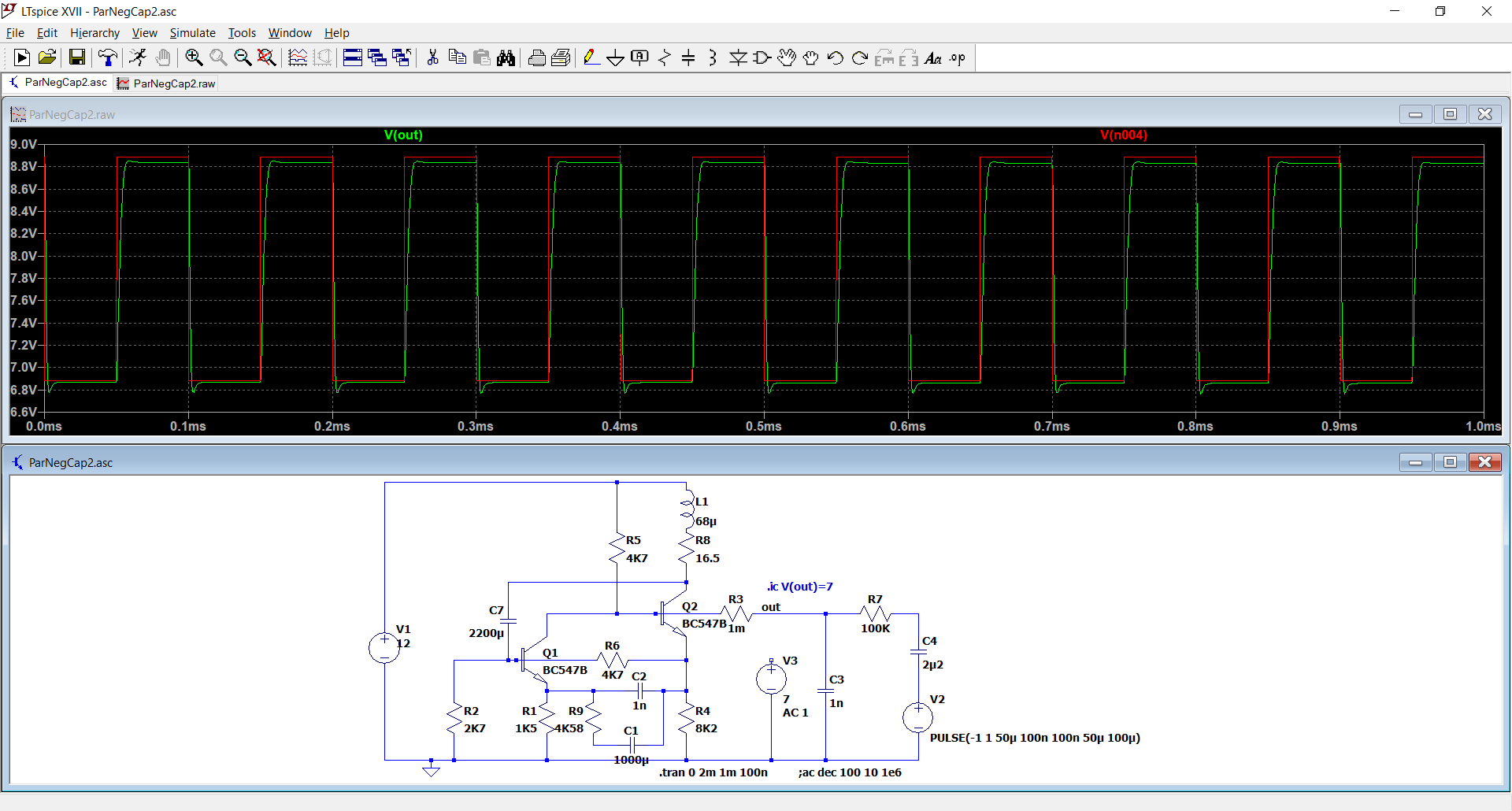
This circuit inverts C2, and the -1nF is connected in // with C3, cancelling it: this can be verified with the time-domain response. The 100K in series with the 10kHz squarewave source has a minimal effect.
In the frequency domain, the magnitude of the current through C3 and -C2 is similar, but the phases are 180° apart:
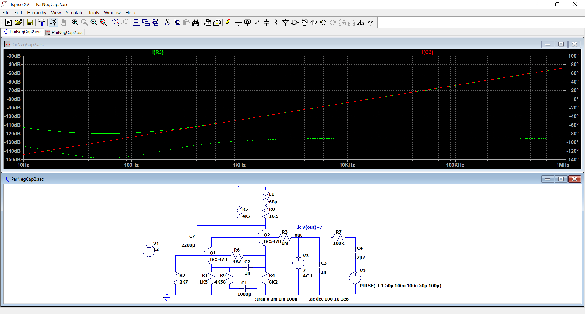
Various components, L1, R8, R9 compensate for the parasitics of the transistors and the bias and load resistors required to make the transistors function normally. Their value needs to be accurate if the positive capacitor has to be 100% cancelled.
Another variant, first in the time-domain:
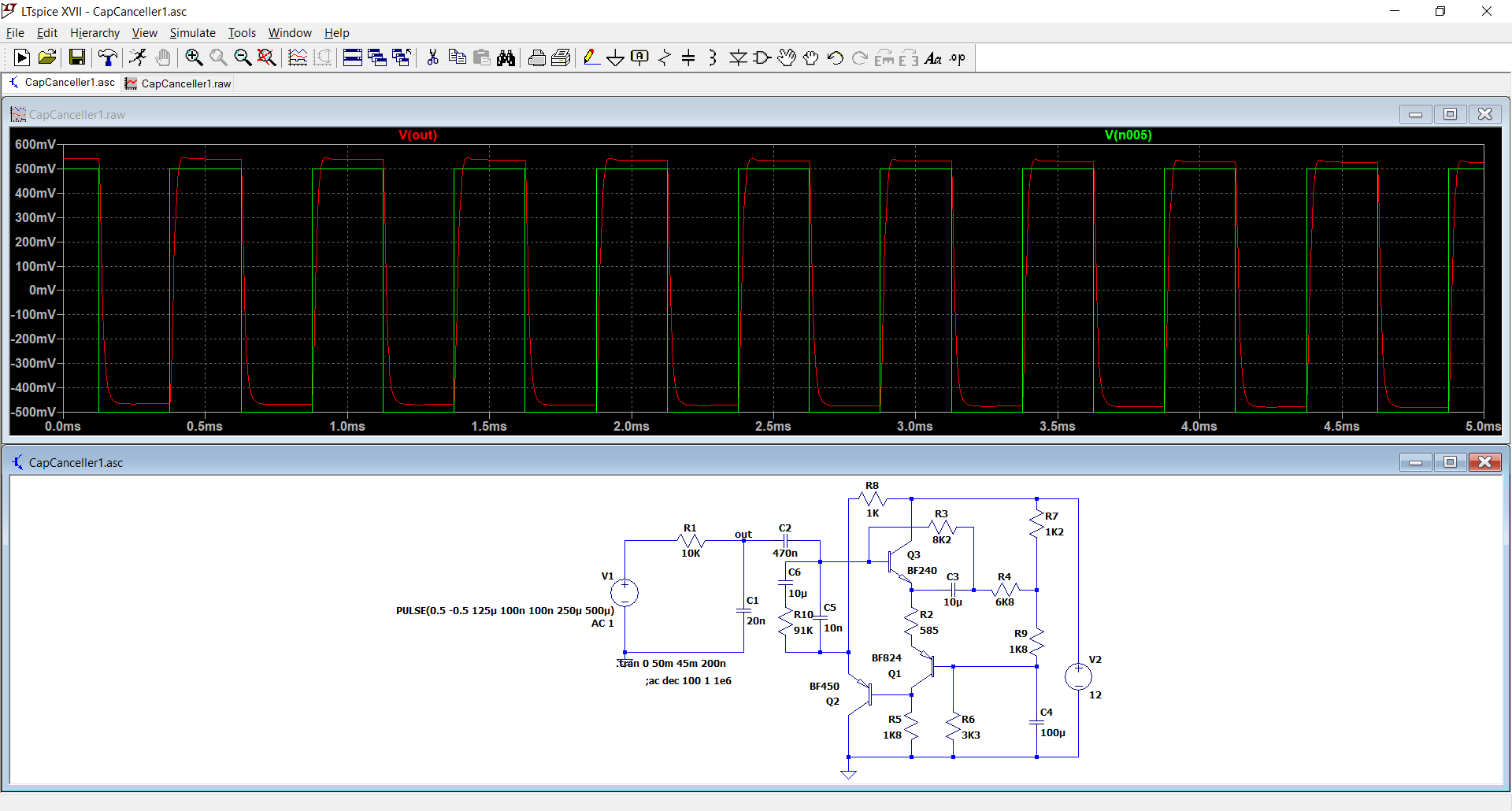
Then in the frequency domain:
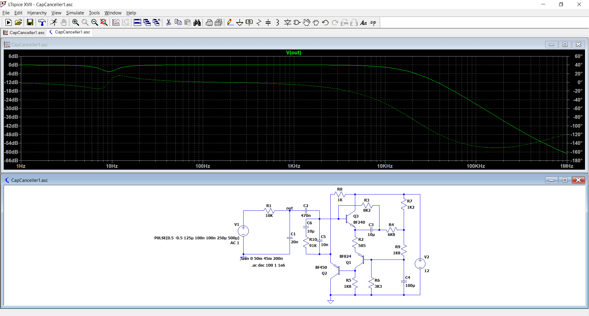
Again, R10 is a compensating component, but something should also be added for higher frequencies; anyway, these are just examples, and the LF blip is caused by too small coupling caps.
Now, the series version, in the time-domain:
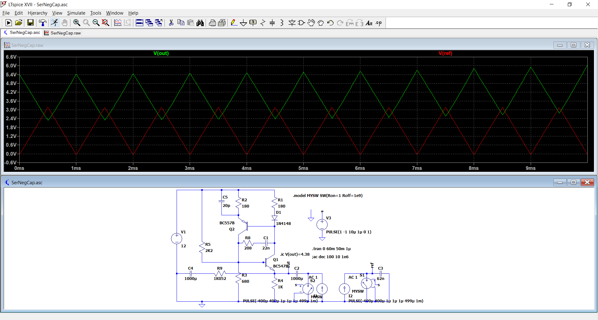
The simulated capacitor behaves exactly like its positive counterpart, the 62nF capacitor but with the phase reversed.
The same in the frequency-domain:
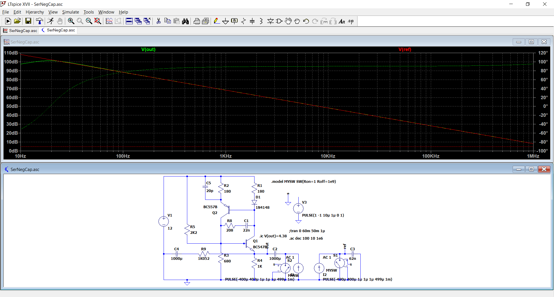
Again, same behaviour but the phases are 180° apart.
Many more implementations are possible, including with "easier" building blocks, like opamps, OTA, etc. and they generally make the job easier because they are more ideal, and do not require compensating components, but with discrete transistors operation remains possible at hundreds of MHz or more.
To summarize: practical negative capacitors come in two varieties:
-Those stable with a load ranging from a short to their nominal values, suitable for parallel operation
-Those stable with a load ranging from their nominal value to infinity, suitable for series operation
To my knowledge, no physical circuit is able to meet those two conditions at the same time, AND present a negative capacitance (but I could be wrong)
Negative capacitors are synthetic, virtual constructions but they find uses in many applications: you have probably already used or built one, maybe unknowingly when it is part of a more complex system.
Like all synthetic, negative components, they are enshrouded in an aurora of mystery.... and this is partly justified.
In fact, negative capacitors exist in two flavours: series and parallel. This may sound surprising: a negative capacitor is just a capacitor having a minus sign in front of its value, and there aren't many ways of doing that: only one is possible.
Thus, from a purely theoretical point of view, negative capacitors are negative capacitors, period. Move along, there is nothing else to see.
From a practical point of view, things are different: if you try to implement a stable, usable negative capacitor, you will need to make a choice.
To understand the distinction, you need to get back to the capacitors association formula's: in parallel, Ctot=C1+C2 and in series, Ctot=C1*C2/(C1+C2).
To be stable, a negative capacitor has to be associated with a positive one and the resulting capacitance has to be positive.
Thus for the parallel case, assuming C2 is the negative one, C1>C2, no surprise there.
For the series case, the numerator C1*C2 will always be negative. This means that the denominator has to be negative too, thus the stability condition is C2>C1, opposite to the previous one.
In addition, the resulting capacitor will have a larger capacitance than any of its components, and it will tend to infinity if the compensation is exact.
The synthetic negative capacitor has no idea about the intentions of the designer or the topology of the circuit it is included in: it reacts according to the capacitance it is loaded with, and if the value is outside its stability range, it will be unstable. A topology stable for C1>C2 is going to be unstable for the reversed condition, and vice-versa.
With a parallel connection, you have to opt for a circuit which is stable for C1>C2, and the opposite for a series configuration.
Parallel negative capacitors are the most common variety: they serve to cancel parasitic capacitances in cables etc. Filters, oscillators also use them.
The series type can be used to cancel the series capacitance of low-capacitance transducers like microphones, to lower the cut-off frequency of some circuits, etc.
Here are two examples of // negative capacitors:
This circuit inverts C2, and the -1nF is connected in // with C3, cancelling it: this can be verified with the time-domain response. The 100K in series with the 10kHz squarewave source has a minimal effect.
In the frequency domain, the magnitude of the current through C3 and -C2 is similar, but the phases are 180° apart:
Various components, L1, R8, R9 compensate for the parasitics of the transistors and the bias and load resistors required to make the transistors function normally. Their value needs to be accurate if the positive capacitor has to be 100% cancelled.
Another variant, first in the time-domain:
Then in the frequency domain:
Again, R10 is a compensating component, but something should also be added for higher frequencies; anyway, these are just examples, and the LF blip is caused by too small coupling caps.
Now, the series version, in the time-domain:
The simulated capacitor behaves exactly like its positive counterpart, the 62nF capacitor but with the phase reversed.
The same in the frequency-domain:
Again, same behaviour but the phases are 180° apart.
Many more implementations are possible, including with "easier" building blocks, like opamps, OTA, etc. and they generally make the job easier because they are more ideal, and do not require compensating components, but with discrete transistors operation remains possible at hundreds of MHz or more.
To summarize: practical negative capacitors come in two varieties:
-Those stable with a load ranging from a short to their nominal values, suitable for parallel operation
-Those stable with a load ranging from their nominal value to infinity, suitable for series operation
To my knowledge, no physical circuit is able to meet those two conditions at the same time, AND present a negative capacitance (but I could be wrong)
Attachments
I'd like to connect a LM317 style 3-term regulator to my (for me) expensive JLSounds USB to I2S converter. It'll drop ~20+ VDC to +5V. Obviously, if the 317 happens to fail short, there goes the JLS board. Could the shunt portion of your tandem regulator be used to make the '317 regulation even better, plus provide a crowbar - with a fuse on the input? How would those two be linked?
All to take advantage of the converter's USB isolation capability. At the moment, I'm running it off USB power. I was thinking of making a new thread, but here it is - almost! Thanks.
All to take advantage of the converter's USB isolation capability. At the moment, I'm running it off USB power. I was thinking of making a new thread, but here it is - almost! Thanks.
You could, but to make the crowbar bullet-proof, you would need to add a power diode (like a 1N400x) across R2 (1 ohm). Note that you also need to provide a 5V reference voltage, and it should be extra-clean (this wouldn't be difficult, since the reference input requirements are modest).
Edit:
If your intention is to use the shunt part only, with a 317 as series regulator, it should be possible too, but this needs a little reflection
Edit:
If your intention is to use the shunt part only, with a 317 as series regulator, it should be possible too, but this needs a little reflection
After all, using a 317 as a series element doesn't look advantageous: it is a fully fledged regulator by itself, and using its internal reference looks problematic, and anyway if the regulator fails, this voltage could go anywhere.
Using the 317 just as a dumb ballast would be possible, but it is relatively noisy compared to a simple transistor, and another voltage reference would have to be found.
Using a 317 augmented with a denoiser-like circuit, together with a standard crowbar (SCR-based) looks like a more sensible solution.
The other option is to go full tandem, and use one of the circuits proposed here (but in their present form, they have no overcurrent or thermal protection, unlike a 317)
- Home
- General Interest
- Everything Else
- I am clearing my attic: here is the legacy thread