Hi all.
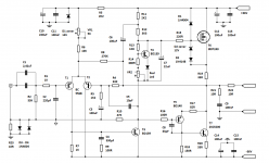
This circuit is a variant of the circuit that develops in the thread "Very simple quasi complimentary MOSFET amplifier" (Ranchu32). This circuit is a hybrid quasi output, with LTP input.
Characteristics.
1. LTP PNP input
2. No miller cap in VAS
3. Shunt compensation before the VAS
4. Phase lead
5. Hybrid quasi output: a nmos top and npn bottom.
What are your comments?
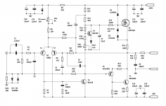
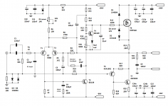
Attachments
It looks an interesting and somewhat different design 🙂
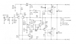
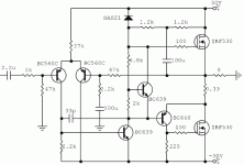
R19 and R20 look like a typo error (33R). D2 zener and D2. Do you need these ? plus they will only clamp in one direction. I can't see D1 ever coming into play.
R10 will change the distortion profile of the whole amp at the expense of limiting the VAS swing... however it can be a trade-off worth exploring for subjective quality 😉
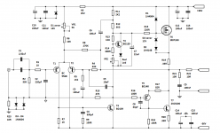
Hybrid quasi output LTP input
The diode is there exactly to prevent the MOSFET from being driven all the way on the positive half cycle.
See post 166 and 169 (ilimzn),in the thread "Very simple quasi complimentary MOSFET amplifier" (Ranchu32).
The diode is there exactly to prevent the MOSFET from being driven all the way on the positive half cycle.
See post 166 and 169 (ilimzn),in the thread "Very simple quasi complimentary MOSFET amplifier" (Ranchu32).
Attachments
OK, thanks. Wouldn't like to say one way or the other on that without actually trying it for real and seeing how it all behaved... but the reason is valid.
Hi nigelwright7557.
See post 162 (ilimzn),in the thread "Very simple quasi complimentary MOSFET amplifier" (Ranchu32).
...."Now, becasue of the unusual nature of a BJT CFP/MOSFET combination, there is actually more that can be done to simplify the design. For one, the R-C-D parallel combo is not necessary. This would be used if the top was a BJT darlington, and it's used to make the crossover region more symmetrical, because for the CFP it's much narrower than that of the darlington. In the case of this amplifier, it's very difficult to do this since the devices are so different. However, it is possible to narrow the Vgs range the top MOSFET works in, by excluding the source ressitor. At the same time, the 'emitter' resistor of the CFP mentioned above should be increased, perhaps to 0.47ohms."
I think this works. What he says iliman matches mosfet Citation 12 circuit.
Member
Joined 2009
Paid Member
Hi Bigun. Thank you.
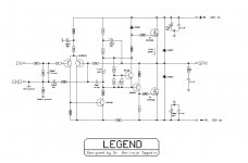
This circuit is of many contributions, Aksa, Ranchu32, ilimzn, vzaichenko and other forum members. Previous circuits like mosfet Citation 12, Legend.
This circuit is intended for those who want to simulate or test.
I will apply the output circuit in updating another circuit that is in the thread "No Miller cap, Double bootstrapping amp".
Regards
Looks interesting. Have you built and tested it? What advantages does this compensation scheme (C5 & R9) over the more conventional miller capacitor?
Member
Joined 2009
Paid Member
Make C12 and C14 larger, 1,000uF if you can. This will ensure that the majority of the speaker currents can circulate on the amplifier board. Allow for some LTP degeneration, even a few ohms will be handy for measuring the relative current flows down the two 'legs'.
Hi Ranchu32.
The R9 + C4 across R7. This circuit does not use miller cap.
“Common emitter configuration is normally used for the voltage amplification stage (VAS), but suffers from Miller capacitance and Early effect, well known parasitic problems related to this solid state topology” (Hugh Dean).
It is replaced by this RC network of compensation. In the opinion of several members of this forum R + C is the better alternative for feedback compensation than Cdoms. It is also known as RC shuntcomp. The other stability components are in other locations, R1 (1k) and C2 (200 pF) and C5 (10pF) phase lead. I've seen long ago in the Arcam A60. I have recently seen in the amplifier vzaichenko. Ostripper also use it in your project supersym.
Before building a prototype as a test, I first want to adjust the circuit. For example it seems necessary to include an R nested feedback.
Regards
Member
Joined 2009
Paid Member
- Status
- Not open for further replies.
- Home
- Amplifiers
- Solid State
- Hybrid quasi output LPT input