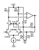
I am looking at a schematic from Cordell's LSK489 app note, specifically figure 6(c) and I am trying to figure out a couple of things:
Do the jfets J3 & J4 need to be of higher Idss, or could LSK489s be used there too?
Could someone help me understand the feedback paths? Specifically:
Why do the gates of J3 & J4 need to be fed with 7Vdc besides the signal feedback?
In case of a unity buffer, could I simply replace R3 with a 1K?
Thank you.
Attachments
Why do the gates of J3 & J4 need to be fed with 7Vdc besides the signal feedback?
In case of a unity buffer, could I simply replace R3 with a 1K?
That's a cascode connection.
Since this is non-inverting, the gain is (1+ R3/R4).
Make R4 large compared to R3 for near unity gain.
Compensation for stability might be required for low gain.
Gate resistors in the jfets may also be a good idea.
Last edited:
Make R4 large compared to R3 for near unity gain.
Thanks rayma.
So it's better if both resistors are 9,1K instead of both being 1K?
That would be ok, and give a gain of x2 or +6dB.it's better if both resistors are 9,1K instead of both being 1K?
If you want a gain closer to unity, make R4 larger, say 50k. That would give around +1.4dB gain.
Be careful to check for HF oscillation.
Last edited:
use a medium Idss, high gm, low Vpinchoff (Vp), device for the two LTP devices.I am looking at a schematic from Cordell's LSK489 app note, specifically figure 6(c) and I am trying to figure out a couple of things:
Do the jfets J3 & J4 need to be of higher Idss, or could LSK489s be used there too?
Could someone help me understand the feedback paths? Specifically:
Why do the gates of J3 & J4 need to be fed with 7Vdc besides the signal feedback?
In case of a unity buffer, could I simply replace R3 with a 1K?
Thank you.
Use a low gm, high Vp, high Idss, device for the two cascodes.
I suggested some years ago for lsk170 & bf244 that the Idss for the cascode:
Cascode Idss should be 2 times [1+the Idss of the LTP].
eg.
for an LTP running at 3mA per side use a 3.5mA to 4mA Idss lsk170a
Add one to give 4.5 to 5mA and then double that to 9mA to 10mA for Idss of the bf244b, or bf244c
From the above you can see that using a high Idss for the LTP that a very high Idss is required for the cascode. I don't know how to measure a very high Idss jFET without risking damaging it.
Borbely tells us to operate jFETs at Vds > 2*Vpinchoff.
The above method should give more than 2*Vp for the LTP Vds.
R.Cordell's circuit is a bit different in that R6:R7 sets the cascode voltage. But the Borbely rule should still be applied.
Check your LTP Vds and compare to Vp
Last edited:
- Status
- Not open for further replies.