Hi,
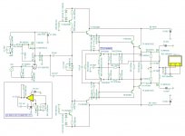
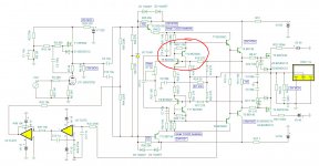
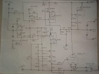
I want to built hybrid tube/ss power amp. My goal is to use no feedback tube voltage stage driving solid-state class AB unity gain buffer. I dont want ss class A buffer - too much heat. So I want to use Hawksford error correction. Attached schematics works in simulator (ss part hasnt been built yet).
I have one problem - do I need DC servo to null output dc offset drift? Where should I connect output of the servo?
Thank you.
Attachments
Pretty good, KCN (potassium cyanide??).
To ensure the two CCS work together, I would disconnect ground points of R38 to R44 and link together to mutually float.
I cannot suggest anything else - it's a very good circuit.
HD
To ensure the two CCS work together, I would disconnect ground points of R38 to R44 and link together to mutually float.
I cannot suggest anything else - it's a very good circuit.
HD
I am not sure if I need those CCS at all.
What about DC servo? Can you please help me, where should I connect output of the DC servo?
Thanks.
What about DC servo? Can you please help me, where should I connect output of the DC servo?
Thanks.
Member
Joined 2009
Paid Member
connect output of the servo to the base of T11
If you want to reduce the transistor count, replace the CCS with split resistor and capacitor from output - good ol' bootstraps
you don't need C11
do you need any diodes on the power rails to ensure the circuit is happy regardless of what sequence the power supply rails come up to full voltage ?
do you need a mute on the tube circuit whilst it heats up ?
Last edited:
Member
Joined 2009
Paid Member
clearly I've no clue how this error correction circuitry takes control of the output stage - that would be the next place I'd look for a control pointConnecting servo to the base of T11 or T10 doesn´t work according to simulation.

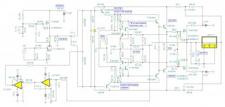
Redesign
I am now using TL431 for the input transistor bias and it works very good. DC servo now works too.
Now how to make boosted rails simply and easily for the EC frontend wihout needing another extra winding or transformer.
I am now using TL431 for the input transistor bias and it works very good. DC servo now works too.
Now how to make boosted rails simply and easily for the EC frontend wihout needing another extra winding or transformer.
Attachments
Hi.
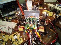
I too have created a hybrid using hollow state as the VAS and solid state as the output stage, with Dr Hawksford's amplified diode circuit with vertical mosfets. I use bootstrap to provide the boosted rails for the HEC. It can be done!! ....and should be done IMO. The triodes I have are very old DHT's, UX201A. These are unique devices and so I made a circuit specific for them. I really only have designed SS circuits before, not much experience with valves but I intend to expand my horizons with the empty glass thingies and I figured this would be a good start.🙂. I used the same amp (stereo) circuit that I made HERE. Like a typical solid state design it is used directly coupled😛. This means that a voltage conveyer had to be used to transfer the signal to the grid/filiment voltage with the plate voltage at 0V, and I used this circuit to add some voltage gain because the UX201A has u of maybe 7. I did use feedback but the FB factor is quite small. But they are very linear and make very wonderful VAS!😀. Because it is directly coupled (except for the input cap of course) it requires a DC servo to correct for drift just like the SS design, and so the DC will balance to within 30mV or so. Overall, the design uses circuit blocks that perform separate functions that work together, input stage and volume control (THAT2162), VAS, output stage, logic control/protection, and so I could adapt the VAS section to use this device. I was initially skeptical but proceeded onto success! 😀. More to come on this project when I get back home. Still on vacation.🙂. HERE is a post with photos. Feel free to utilize any ideas that might apply to your project, as the goal is to make it work, no? 😀
I too have created a hybrid using hollow state as the VAS and solid state as the output stage, with Dr Hawksford's amplified diode circuit with vertical mosfets. I use bootstrap to provide the boosted rails for the HEC. It can be done!! ....and should be done IMO.
The triodes I have are very old DHT's, UX201A. These are unique devices and so I made a circuit specific for them. I really only have designed SS circuits before, not much experience with valves but I intend to expand my horizons with the empty glass thingies and I figured this would be a good start.🙂. I used the same amp (stereo) circuit that I made HERE. Like a typical solid state design it is used directly coupled😛. This means that a voltage conveyer had to be used to transfer the signal to the grid/filiment voltage with the plate voltage at 0V, and I used this circuit to add some voltage gain because the UX201A has u of maybe 7. I did use feedback but the FB factor is quite small. But they are very linear and make very wonderful VAS!😀. Because it is directly coupled (except for the input cap of course) it requires a DC servo to correct for drift just like the SS design, and so the DC will balance to within 30mV or so. Overall, the design uses circuit blocks that perform separate functions that work together, input stage and volume control (THAT2162), VAS, output stage, logic control/protection, and so I could adapt the VAS section to use this device. I was initially skeptical but proceeded onto success! 😀. More to come on this project when I get back home. Still on vacation.🙂. HERE is a post with photos. Feel free to utilize any ideas that might apply to your project, as the goal is to make it work, no? 😀Attachments
Last edited:
Your amplifier is too complex for my brain 🙂. Definately nice execution! I bet it sounds great.
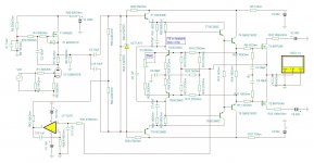
In Bob Cordell´s book "Designing Audio Power Amplifiers" he writes:
"Transistor T8 is mounted on the heat sink to provide thermal feedback. Thus, about half
of the total bias spread is compensated by the temperature of the heat sink. T8 is preferably a fast TO-92 transistor embedded in a hole in the heat sink. The wiring to this
transistor should be fairly short so as to avoid parasitic oscillations."
Now if I implement CFP for T8, should be both CFP transistors T8 and T10 mounted on the heatsink for temp compensation?
Thanks.
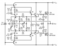
Attachments
Hi.
Yeah, as a whole it kinda is. But breaking it down for example, the clipping detection is right from Rod Elliot's site as is the DC detection circuit. The volume control circuit for the THAT2162 is right from the datasheet. It's just that I used many SMD parts crammed on to a 4 layer PCB.😛. I found an old drawing from a simpler circuit (here) that I made from AF components. It worked well. So I updated it in the latest version with faster devices and extra cascode stages, and with some trial and error with the pole/zero values to keep stable, I could go as low as 10 to 15mA for bias without issues. I use a fixed resistor for bias (Rb). Notice that the input signal is only AC, with zero volts DC, and with the bootstrap, no extra rail voltage is needed. This greatly simplifies things I think.🙂
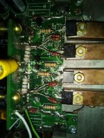
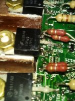
The error amplifying device is the only one that needs thermal coupling not the CFP one. But, with the vertical mosfets, the temperature coefficient is related to Gm and for these devices, Gm drops very significantly lower at low current, at a few hundred mA, decreasing exponentially. This why the error signal voltage is logrithmic, essentially replacing the missing Gm with dV/dT of error signal voltage. The close up photo shows the small SMD transistor mounted under the drain pin to sense temperature. I found that with mosfets it is easy to overcompensate for the thermal drift, so sampling further from the device seems to better track the bias. It doesn't have to be as accurate as for the Darlington bipolar. Gm for bipolar is higher at low current around class AB bias, and are more sensitive to bias fluctuating with temperature particularly because of two cascade transistors on the same die.
Yeah, as a whole it kinda is. But breaking it down for example, the clipping detection is right from Rod Elliot's site as is the DC detection circuit. The volume control circuit for the THAT2162 is right from the datasheet. It's just that I used many SMD parts crammed on to a 4 layer PCB.😛. I found an old drawing from a simpler circuit (here) that I made from AF components. It worked well. So I updated it in the latest version with faster devices and extra cascode stages, and with some trial and error with the pole/zero values to keep stable, I could go as low as 10 to 15mA for bias without issues. I use a fixed resistor for bias (Rb). Notice that the input signal is only AC, with zero volts DC, and with the bootstrap, no extra rail voltage is needed. This greatly simplifies things I think.🙂
The error amplifying device is the only one that needs thermal coupling not the CFP one. But, with the vertical mosfets, the temperature coefficient is related to Gm and for these devices, Gm drops very significantly lower at low current, at a few hundred mA, decreasing exponentially. This why the error signal voltage is logrithmic, essentially replacing the missing Gm with dV/dT of error signal voltage. The close up photo shows the small SMD transistor mounted under the drain pin to sense temperature. I found that with mosfets it is easy to overcompensate for the thermal drift, so sampling further from the device seems to better track the bias. It doesn't have to be as accurate as for the Darlington bipolar. Gm for bipolar is higher at low current around class AB bias, and are more sensitive to bias fluctuating with temperature particularly because of two cascade transistors on the same die.
Attachments
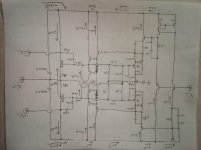
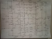
 Just as well, here is the expanded implementation I am using now, and an update on the VAS with the triode.🙂
edit: it seems the pics posted upside down. Hmm

Attachments
Last edited:
You could try smth like this for the frontend.The second link is a version of a phono preamp which was able to reproduce up to 25khz square signals(480khz sinus) through the antiriaa and very low impedance riaa network.You could drive high power devices with low distortions with this arangement.
https://www.diyaudio.com/forums/ana...v2-phono-riaa-preamplifier-2.html#post5271628
https://www.diyaudio.com/forums/analogue-source/255149-unu-pnono-riaa-mm-preamp.html#post5485527
https://www.diyaudio.com/forums/ana...v2-phono-riaa-preamplifier-2.html#post5271628
https://www.diyaudio.com/forums/analogue-source/255149-unu-pnono-riaa-mm-preamp.html#post5485527
Hi
I believe from Mr Cordell's book, each gate Zobel filter should go from gate to drain, not to GND. The idea is to dampen the mosfets internal components from creating an oscillator. Also the ballast resistors should be on the source of mosfets, not the drain.
I believe from Mr Cordell's book, each gate Zobel filter should go from gate to drain, not to GND. The idea is to dampen the mosfets internal components from creating an oscillator. Also the ballast resistors should be on the source of mosfets, not the drain.
Last edited:
Mosfet zobel filter goes to ground.
Two 0.1R resistors on drains are just for simulating purposes, so I can measure current going through mosfet. Interesting is, Nelson Pass mentions source degeneration resistors are another source of distortion (higher order), in his XA25 he doesnt use them.
He says:
"That effect is somewhat spoiled by degenerative source resistance used to constrain the 'personality' of the devices. The removal of this form of feedback is an important element in the performance of the XA25. It is accomplished by new approaches to stabilizing gain and bias of push-pull Fets. This gives a lower output impedance, more gain and lower spectral content of distortion as evidenced by measurements. But the more important factor is the difference it makes to the music. We observed this difference in listening tests some years ago. Degeneration removed some of the organic quality to the sound. So it became the subject of further development work."
Attachments
Hi.
The XA25 output stage is quite a bit different than the Amplified Diode circuit by Hawksford. It sounds like he is trying to reduce output Z without increasing feedback factor of amp, or something like that. The ballast resistors in the Amplified Diode circuit are within the feedback/feedforward network and effectively become part of the device. It's main function is to reduce the percentage difference of the Gm of the N-ch and P-ch mosfets, which are not the same. This, and the small pot between emitters of the error amplifier help to provide better symmetry to the error signal. Also, without the ballast source resistors the thermal bias stability will become difficult to stabilize. XA25 output stage appears to be class A or very high bias class AB. The source resistors do not have much effect here, which is why Mr Pass discarded it. I doubt he would have removed it if it were important in his design. Low bias class AB, push pull arrangement has different parameters.
Figure 5 in Mr Cordell's paper on E C power amp explains the internal reactive components of a mosfet, and how it forms an oscillator. Also, how to dampen this oscillator from bursting out in RF oscillation under load. If not properly damped, it will burst out with 10 or more MHz frequency under heavy conductance and cause destruction. In my experience I have found that the zero works better when placed from gate to drain as in the paper.
I will point out that in my experience, circuit layout is important due to high frequency operation, symmetrical layout is best, at least for the EC amplifier part. I have had great success with this circuit although I don't see it applied much here on the forum.
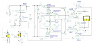
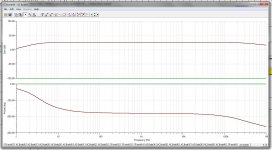
Thank you for your help. I have changed schematics according your recommendations. I have to add series resistor to bootstrap capacitor to eliminate low frequency bump about 10 Hz.
Do you think circuit is now ready to be built?
Do you think circuit is now ready to be built?
Attachments
- Status
- Not open for further replies.
- Home
- Amplifiers
- Solid State
- Hybrid Mu Follower Poweramp with Error Correction