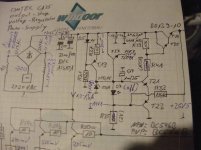
In the attachment the associated schematic diagram (both diagrams nearly identical - the only difference is the polarity).
This voltage regulators feds only the offset servo (TL071), the VAS-stage and the 3V8 regulator for the input stage, but not for the output buffer.
The whole diagram I have posted here (post #25) :
Omtec Mono Power Amplifier "CA 25" (CA25) - Schematic wanted
I understand, how works the small 15V regulator part for the offset servo TL071:
T19/20, R37/38, LED D5/D6 and R31/R32 create a current source (appromixately 3-3,5mA) for the zener diode ZD1/ZD2 (15V).
This zener diode is not only connected with the base of T27/T28 which supplies by the emitter ~14V3 to PIN4&7 of TL071.
This zener diode is also connected to the following parts arround the main regulator section consisting of darlington transistor function T25+29/T26+30:
1) base T21/22 and
2) anode LED D7/D8,
This both LED's emits only a very faint red light. I don't think, that is correct. But there are no faulty transistors and resistors.
Some questions rises up:
Which task do these parts have together with R35/R36 and R33/R34 ?
and additional I want to know, which voltage regulation range can be realized
and how stable must actually be the voltage at varying loads on the emitter of T29/T30 ?
What could have been the reason to prefer this circuit topology?
Maybe a redesign of this regulator circuit is necessary for a proper resp. better operation.
Thank you very much for advices.
I wish all diyaudio members a Merry Christmas.
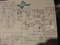
Attachments
Last edited:
T21 and T23 are sort of long tailed pair without a tail.The zener voltage at base T21 is compared to Vz-2xVbe at the base of T23.The voltage on base T23 comes from the output voltage divider R33,R35. The LED is a limiter like the two anti-parallel diodes in an ordinary pair with a tail.
Mona
Mona
Thank you.
I can use now the following basic equations for R33 and R35 according this article
Voltage And Current Regulators
R33 + R35 = V IN - V OUT / I B * 10 - where I B is determined by ...
I B = I OUT / h FE ( T25 * T29 ) ... (assume gain of 1000), so ...
I OUT = 200mA
I B = 200µA * 10 = 2mA
VIN - VOUT = 30V5 - 25V5 = 5V
R33 + R35 = 5V / 2mA = 2,25k
Last edited:
The voltage check by variation of R33/34 both at the regulator output from the model CA60 output and various nodes provide the below mentioned results (please note, that the input voltage and the output voltage at CA60 is higher as at the model CA25):
R33/34 0K5 1K 2K 3K6* 5K4
Node____________________________________________________
Input Voltage C, T29/30 45V5 45V5 45V5 45V5 45V5
Output Voltage E, T29/30 42V 42V 42V 42V 35V
B, T23/24 and K, D7 (LED) 32V 28V 21V 15V 9V5
E, T23/24 and E, T21/22 23V 20V 14V3 14V 10V2
B, T21/22 and K, ZD1 (ZPD15) 15V 15V 14V9 14V5 10V9
3K6* for R33/34 is the genuine condition (originale state)
This means, my estimate and the description in post #2 can not really be correct.
Last edited:
Good advices, thank you very much.
The schematic is exact according the PCB of both CA25 and CA60, thus it is possibly a design error in this circuit from its developer, Mr. Manfred Baier.
But I am not sure - therefore one question remains:
Are there any advantage concerning SNR by the use of a positive feedback instead the usually used negative feedback in these discrete voltage regulator ?
Last edited:
In the meantime I don't believe, that there is any advantage concerning SNR by the use of a positive feedback, because I read underGood advices, thank you very much.
The schematic is exact according the PCB of both CA25 and CA60, thus it is possibly a design error in this circuit from its developer, Mr. Manfred Baier.
But I am not sure - therefore one question remains:
Are there any advantage concerning SNR by the use of a positive feedback instead the usually used negative feedback in these discrete voltage regulator ?
http://www.ti.com/lit/an/snva020b/snva020b.pdf
(go to the following section: "7.3 feedback") this:
Feedback is used in all voltage regulators to hold the output voltage constant. The output voltage is sampled through a resistive divider (Figure 6), and that signal is fed back to one input of the error amplifier. Since the other input of the error amplifier is tied toa reference voltage, the error amplifier will supply current as required to the pass transistor to keep the regulated output
at the correct DC voltage. It is importante to note that for a stable loop.
negative feedback must be used. Negative feedback (sometimes called degenerative feedback) is opposite in polarity to the source signal
(see Figure 7).
Because it is opposite in polarity with the source, negative feedback will always cause a response by the loop which opposes any change at the
output. This means that if the output voltage tries to rise (or fall), the
loop will respond to force it back to the nominal value.
Positive Feedback occurs when the feedback signal has the same polarity
as the source signal. In this case, the loop responds in the same direction
as any change which occurs at the output. This is clearly unstable, since
it does not cancel out changes in output voltage, but amplifies them.
It should be obvious that no one would intentionally design positive feedback into the loop of a linear regulator, but negative feedback becomes positive feedback if it experiences a phase shift of 180 °
The only reason that could have been here to have decided for a positive feedback is the follow:
At higher frequencies the positive feedback turns automatically in the negative feedback.
But that's ultimately also hard to believe for me.
Last edited:
"long tailed pair without a tail"
Sorry, but this is not positive fb, it is negative as it should be,
otherwise the output voltage formula would also not apply.
Ketje is correct in writing that the error amplifier is a "long
tailed pair without a tail". Sometimes a transistor pair like
this is called "Rush cascode". Jan D. has shown a similar
but high voltage regulator somewhere.
I guess the regulator is working and no need to "improve" it.
LEDs D7, 8 are only good to limit base emitter voltage of the
error amps and should not light up under normal conditions.
Of course I can not decide your or Ketjes schematic is true as
seen or corresponds to what is found inside the Omtec amp.
Why reply after one year ? I was looking for "long tailed pair
without a tail" and found only three results on Ggl, two of them
in this forum and the third in Wireless World April 1975 "A Novel
Class B Output?" that I already knew. This one is referenced here:
https://www.diyaudio.com/forums/sol...ossover-distortion-1975-a-20.html#post5338753
.....I was looking for "long tailed pair
without a tail" and found only....
How can a long-tail be tail-less?
The topology is old. Here is a report of a sighting in a 1967 book; sorry, I no longer know what book.
Hello,
maybe i find the solution.
The re-engineering from @tiefbassuebertr seems to be okay. I think that T25/26 have the wrong polarity (npn, pnp) and the wrong connection.
When the Collcetor of the BC Transistor feed the Base of the BD Transistor the function of the regulation is given (a falling voltage at the output opens the tail-transistors and so opens T25/26 which drives T29/30).
Hope that this is the right solution and helps Omtec owners.
Best regards
Michael
Schematic as corrected in post 5 is working.
Your proposal is working also, because you made it the other way round, with
reversed differential connection and collector output by complementary darlington.
Stability issues may be different though.
Your proposal is working also, because you made it the other way round, with
reversed differential connection and collector output by complementary darlington.
Stability issues may be different though.
Hello,
yes, that´s right.
My intention was to check if there was any fault by transfering the layout into a circuit diagram (see the thread: Omtec Mono Power Amplifier "CA 25" (CA25) - Schematic wanted). And the circuit in post #5 is, in my sight, not the solution. But you´re right, it works.
I am not 100% sure, the final check may be to measure the voltages on a omtec-pcb.
The advantage is a higher open loop gain (the differential amp and the transistor T25/26) given a higher feedback and a lower output impedance.
I am not owning omtec amplifiers, for me it´s fun to analyse circuits and learn from great audio-designers (omtec amplifiers have a high reputation here in germany, also the designer Mr. Manfred Baier).
Best regards
Michael
In my understanding the original question was : how does this regulator work.
We can not be sure Tief extracted the schematic as it is in reality, we can only
reply to what he writes here.
If you know more just let us know.
In general, asking for schematics of obscure german amps manufactured by a
single person 40 years ago in an international forum will lead to nowhere.
In daily life I just repair these amps and do not care about the intentions of any
designer in the past.
- Home
- Amplifiers
- Power Supplies
- How works Manfred Baier's Voltage Regulator in his OMTEC Power Amplifiers CA25+CA60 ?