Actually the title may be misleading - I don't need help screwing up my SP-10, I've done that myself.
I bought an SP10 that didn't have a PSU. I built a PSU according to the design by MP Barney. It's a clever design that starts the 32.5VDC a bit later than the 5V owing to a larger capacitor on the 32V regulator. I've built one of these previously and it worked like a charm.
HOWEVER, I'm an idiot: I connected the 32.5V supply to the 5V connector on the table, and vice versa. I corrected it but the table won't run. I suspect I've screwed up the logic circuit by supplying it with 32V instead of 5V.
I don't have the slightest idea where to start troubleshooting. Any suggestions will be appreciated.
EVEN BETTER would be someone who would do the repair for me. Of course I'd pay the going rate for this work. If you're willing to tackle this, please drop me a PM or email at whirsch@indy.rr.com
Thank you.
Last edited:
Yes, the brake engages when the power is applied. The speed LEDs are working and can be changed by the corresponding button.
I'd still welcome ideas for where to begin. This table may be totally screwed up but it could be an opportunity for me to learn more about digital circuits. Anything I learn I will share back on this thread so it might help others.
Thanks.
Thanks.
....SP-10 .... a PSU according to the design by MP Barney. .... ideas for where to begin.
Maybe post links to:
SP-10 circuit
MP Barney circuit
If you're lucky just some of the TTL logic went. Subs are:
SVM53200 - 74LS00 x3
SVM53273 - 74LS73 x7
SVM53293 - 74LS93 x2
SVM5943 - 74LS03 x1
SVM53204 - 74LS04 x1
SVM53210 - 74LS10 x2
The 53273 and 53200 seem the most susceptible to over-voltage, though it depends.
If you change IC8 you'll likely need to change R221 to 1k as the loading is different, likewise change R261 to 1k if either IC9 or IC10 are changed. Last, if IC 11 is changed you may need to add a 22k resistor from pin 3 to +5V as it's an open collector output.
You can either shotgun them all or test one-by-one. Either way I suggest using sockets as the boards aren't likely to stand up well to multiple reworks, and I've seen more than a few that couldn't stand up to a rework at all.
If one-by-one I recommend measuring the current on the +5V rail. Each chip should increase current by no more than around 20mA max. If one increases by more it's bad and should be replaced. Total draw on the +5V rail should be around 250mA. You can insert the chips one at a time, powering on after each to check the current.
If you're a scope you can trace the clock through the logic. The service manual has waveform callouts for nearly every chip so it's not difficult to infer what should be seen.
Also note that the motor should run without a clock. It will steadily increase to maximum speed as the PLL won't lock. However IC8 needs to be functioning and your +5V rail needs to be close to proper voltage, which it likely isn't due to the failed logic drawing excess current. This is one of those scenarios where you hope the aftermarket PSU isn't drastically over spec'd.
Yes, the brake engages when the power is applied. The speed LEDs are working and can be changed by the corresponding button.
I would expect lots (all) of the 74logic to fail with 33v down its snozzle, but the speed lights are run on the same 74logic too, there's no doubt that maybe just one or two key 74logic chips are blown , but I still say you've got more chance of zapping them all or none at all.
How long was it applied for ?
Do you know if this was a working unit before you applied your killer PSU ? 😕
32V on 5V line is complete death to the 5V stuff unless there was a crowbar protection circuit (in which case the 32V supply may be toast). TTL has an absolute maximum supply voltage of about 7V and the inputs are only rated to 5.5V. Standard procedure after this sort of damage is replace all semiconductors on the pcb, its less hassle than trying to save anything (which may be borderline anyway).
32V on 5V line is complete death to the 5V stuff unless there was a crowbar protection circui
But he's saying 33/45 still works as intended , and that's IC 11/12 (at least on a mk2), my scan is a bit murky but looks like a triple 2input nand gate and a 74LS04
I don't see anywhere he says any speed works as intended.
You'd think it'd nuke them all but it usually doesn't. Ultimately I'd replace all the TTL ICs, but it is handy to know which ones bit it as that helps identify areas that may be problematic in downstream circuits.
You'd think it'd nuke them all but it usually doesn't. Ultimately I'd replace all the TTL ICs, but it is handy to know which ones bit it as that helps identify areas that may be problematic in downstream circuits.
I don't see anywhere he says any speed works as intended.
Not the speed, the speed lights (and their control)
The speed LEDs are working and can be changed by the corresponding button.
First let me thank everyone for jumping in with great information! Second my apologies for being missing in action for the past couple days. We're in the process of downsizing our house and it's been a hectic couple days - audio fun has been put on the backburner.
Attached is the schematic for the PSU that I built. I have built this previously and successfully operated an SP10 for a couple years with it.
Also attached are the schematics for the SP10.
I'm inclined to try replacing all the ICs and testing the transistors on the logic board. I REALLY appreciate the list of substitutions for the ICs. I know the subs for the transistors and will list them later.
Attachments
I seem to have similar issue one a logic board from a sp10 mrk2 that i bought off flea bay in a not working condition but cosmetically decent condition sans psu which wasnt an issue as i have a spare after making a slightly improved more modern diy effort.
Switching the unit on i can see the 33 led is functioning and i can select different speeds but when i press start all i get is the platter spinning out of control !!
Using a working unit as a donor i have swapped the control and drive pcbs into the working deck and they seem good but the logic board seems to be the issue possibly
Going through the horizontal waveforms from left to right at the top of the circuit diagram and a couple of the test points i have using a borrowed oscilloscope i no longer have in my possession i got the following :
TR201 nothing
TR202 nothing
TR203 nothing
TEST POINT P3 (IC1 + JUNCTION OF R215 + R215) : 4.7V (SHOULD BE 0.7V)
TEST points at IC8: pin 13 + 14 listed on the logic diagram that shows the circuit traces were also out.
IC3: PIN 5 looks normal
IC4: PIN 14 looks normal
IC5: PIN 1 looks normal
IC6: PIN 14 nothing
IC5: pin5 +junction of IC14: pin 9 unsure
STROBE ic - didnt check as i removed fuse from 140v line in psu but in hindsight i wish i had ......
Waveforms listed vertically on right hand side of the diagram from top to bottom:
IC16: PIN 1 + junction of IC7😛in 1 + ic14 looks normal
IC16: PIN 2 + JUNCTION OF IC 7: PIN 12 LOOKS NORMAL
IC16: PIN 6 + junction of IC 15: pin 2 looks normal
IC16: pin 8 + junction of IC 15 pin 4 NOTHING
IC 15: pin 11 that feeds E12 onto CONTROL pcb NOTHING
Second row of horizontally listed waveforms below the diagram from left to right:
IC 5: PIN 8 + junction of IC13: pin 12 NOTHING
IC10: PIN 5 + TR220 NOTHING
IC9: PIN 9 +junction of IC 10: pin 1 NOTHING
IC10: PIN 12 + junction of IC15: pin 9 NOTHING
Tested the motor windings against a working motor and they seem good thankfully.
I had thought that the lack of waveforms around IC15 was due to a bad IC around 9 + 10 but having changed them and their appropriate loading resistors thanks to @JP here and Nick on the Audiotalk forum but nothing changed in the platter spinning out department.
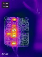
Also swapped out ICS 12 + 7 as they seemed to be a little hotter than their local buddies using a small thermo laser FLIR camera but not as hot as the ones @JP recorded. (i got a normal temp as around 25 degrees celsius and the hotter ones were around 28-30 degrees c with an ambient scottish room temp of 18 degrees c ). There was no change after swapping these out.
Current being used by the logic board alone was around 180ma and then 220ma when plugged in to the rest of the deck.
Sadly the traces below IC11 didnt take well to me removing the IC and about four of the traces from the top of the board shat the bed and turned to dust which meant i had to make a bunch of jumpers to make it right again (IC 11 i tried to take out whole instead of snipping the legs off one by one and taking out the legs one at a time which seems to srtess the board a lot less). The board itself seems to have light brown patches around the solder mask and the traces which might be the issue as the other pcbs ive seen dont have the light brown patches and seem a bit tougher. Turns out it was a waste removing that IC which was a shame but hey ho.
The clock seems to be working ok as i can use a multimeter to read the 3.47mhz at IC2: pin1 which is something at least 😀
Before i go snipping out some more of the original ICS i was wondering what to test next as i feel like a butcher right now when i really wanna feel like a tech .... ?
I have a bunch of the 74LS chips on hand and also some of the KSC1815 trannies on the way and was thinking maybe IC8 + IC15 could be an issue ?
Switching the unit on i can see the 33 led is functioning and i can select different speeds but when i press start all i get is the platter spinning out of control !!
Using a working unit as a donor i have swapped the control and drive pcbs into the working deck and they seem good but the logic board seems to be the issue possibly
Going through the horizontal waveforms from left to right at the top of the circuit diagram and a couple of the test points i have using a borrowed oscilloscope i no longer have in my possession i got the following :
TR201 nothing
TR202 nothing
TR203 nothing
TEST POINT P3 (IC1 + JUNCTION OF R215 + R215) : 4.7V (SHOULD BE 0.7V)
TEST points at IC8: pin 13 + 14 listed on the logic diagram that shows the circuit traces were also out.
IC3: PIN 5 looks normal
IC4: PIN 14 looks normal
IC5: PIN 1 looks normal
IC6: PIN 14 nothing
IC5: pin5 +junction of IC14: pin 9 unsure
STROBE ic - didnt check as i removed fuse from 140v line in psu but in hindsight i wish i had ......
Waveforms listed vertically on right hand side of the diagram from top to bottom:
IC16: PIN 1 + junction of IC7😛in 1 + ic14 looks normal
IC16: PIN 2 + JUNCTION OF IC 7: PIN 12 LOOKS NORMAL
IC16: PIN 6 + junction of IC 15: pin 2 looks normal
IC16: pin 8 + junction of IC 15 pin 4 NOTHING
IC 15: pin 11 that feeds E12 onto CONTROL pcb NOTHING
Second row of horizontally listed waveforms below the diagram from left to right:
IC 5: PIN 8 + junction of IC13: pin 12 NOTHING
IC10: PIN 5 + TR220 NOTHING
IC9: PIN 9 +junction of IC 10: pin 1 NOTHING
IC10: PIN 12 + junction of IC15: pin 9 NOTHING
Tested the motor windings against a working motor and they seem good thankfully.
I had thought that the lack of waveforms around IC15 was due to a bad IC around 9 + 10 but having changed them and their appropriate loading resistors thanks to @JP here and Nick on the Audiotalk forum but nothing changed in the platter spinning out department.
Also swapped out ICS 12 + 7 as they seemed to be a little hotter than their local buddies using a small thermo laser FLIR camera but not as hot as the ones @JP recorded. (i got a normal temp as around 25 degrees celsius and the hotter ones were around 28-30 degrees c with an ambient scottish room temp of 18 degrees c ). There was no change after swapping these out.
Current being used by the logic board alone was around 180ma and then 220ma when plugged in to the rest of the deck.
Sadly the traces below IC11 didnt take well to me removing the IC and about four of the traces from the top of the board shat the bed and turned to dust which meant i had to make a bunch of jumpers to make it right again (IC 11 i tried to take out whole instead of snipping the legs off one by one and taking out the legs one at a time which seems to srtess the board a lot less). The board itself seems to have light brown patches around the solder mask and the traces which might be the issue as the other pcbs ive seen dont have the light brown patches and seem a bit tougher. Turns out it was a waste removing that IC which was a shame but hey ho.
The clock seems to be working ok as i can use a multimeter to read the 3.47mhz at IC2: pin1 which is something at least 😀
Before i go snipping out some more of the original ICS i was wondering what to test next as i feel like a butcher right now when i really wanna feel like a tech .... ?
I have a bunch of the 74LS chips on hand and also some of the KSC1815 trannies on the way and was thinking maybe IC8 + IC15 could be an issue ?
I don't see a callout for P3. IC8 I think you mean pins 12 and 13. Those are flip flop outputs so if the start/stop button works there has to be something there.
Before getting in to the weeds on all this though, do you have a good FG signal? Control circuit test point F. At 33.3 you should see 105.5Hz sine there.
There's a fast and slow run-away. Fast it'll hit a couple hundred RPM in just 2-3 seconds, while slow will take 4-5 seconds to hit around 100 RPM. The former typically indicates an FG signal issue while the latter usually indicates a missing clock.
- Home
- Source & Line
- Analogue Source
- How to Screw up The SP-10: Help needed...