Hello,
I've got a question concerning the biasing of a non-inverting op amp, In my schematic I have a voltage reference point at 1/2 of the supply voltage. What value of the biasing resistor will give me the best noise and overall performance for a certain op amp. What specifications of the op amp should be taken into account and in what way do they define the best biasing resistor value? And what is the approach when biasing an emitter follower to the same voltage reference point?
I've got a question concerning the biasing of a non-inverting op amp, In my schematic I have a voltage reference point at 1/2 of the supply voltage. What value of the biasing resistor will give me the best noise and overall performance for a certain op amp. What specifications of the op amp should be taken into account and in what way do they define the best biasing resistor value? And what is the approach when biasing an emitter follower to the same voltage reference point?
Best if you draw it.
Non inverting means you are biasing the input the signal will be applied to and so the impedance of the bias resistor/network has to be considered.
Another consideration is whether the opamp is FET or Bjt as the Bjt (if it is say a 5532) will draw current from the bias network. The FET type won't.
An emitter follower give a low impedance reference (not always needed) and so you have to choose an appropriate bias resistor to be part of the required input impedance.
What are you trying to do ? and what opamp are you using.
As the voltage reference point will presumably be AC bypassed the resistance values won't have much effect on noise.
I've drawn it. I was asking what determines the value of R-bias (on the schematic) when the designer wants to optimize overall performance (noise, stability, distortion etc) ? In my case, it isn't a buffer, so the input impedance (determined mainly by R-bias) doesn't need to be high at all cost. I just want to get the best performance out of an op amp.
Attachments
R-bias will generate thermal noise, but the source may attenuate this. You will need to provide any input bias current needed by the opamp, as Mooly says.
The values of the feedback resistors may have a greater effect on the opamp performance.
The values of the feedback resistors may have a greater effect on the opamp performance.
R bias must be such that its value in serial with either R3 or R4 will
be equal to R2 , assuming R3 = R4.
If the op amp has BJT NPN input differential , the biasing current
will be drained through R3 , while it will be drained from R4 if it has
BJT PNP input differential.
With a bipolar inputs op amp , the biaising current is low ,
typicaly 200nA for a NE5532/5534 , yet, the current through
the voltage divider R3/R4 must have a significantly higher value,
about one hundreds time more at least.
As pointed by Mooly , this is not the case with fet inputs op amps.
JFET input opamps have such low input current that you can ignore it.
For BJT input amps you want R-bias+(R3+R4)/2 = R2 for minimum offset due to input current. However, as the offset is likely to be much smaller than errors in R3 and R4, it doesn't really matter unless you are running other opamps from the same reference point.
You still haven't told us what you are trying to achieve.
Well, it was more of a theoretical question, rather than anything in particular. Thank you all for the responses, it was really helpful. One last question, though: If biasing a bipolar transistor (emitter follower configuration) through its own R-bias to the ground reference point, what is a good value for R-bias. How does it depend upon the gain of the transistor and its load?
Not much i guess.. they have a voltage gain of approximately 1 and a current gain which depends on the transistor used. They're generally used for impedance transformation (i.e. buffering). And the output is in phase with the input. That's about as wide as my knowledge on the topic spreads.
OK, you probably know enough to calculate the effect of base resistor on an emitter follower. Think about emitter current (what sets that?) and base current (how is that related to emitter current?). Ohm's Law is your friend.
What do you mean by 'the effect of base transistor on the emitter follower'? The resistance seen at the base of the transistor is (transistor's current gain)*(the load resistance), right? And the input resistance of the buffer is (the aforementioned resistance) in parallel with R-bias, right? My question was what is a good ratio between the two? Should they be equal? Or should R-bias be many times smaller that the effective resistance at the base?
I think everyone has answered it all...
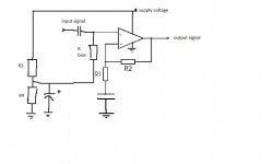
In your diagram,
Rbias determines the input impedance that the signal source will see providing that the cap across R4 is relatively large to all signal frequencies. If Rbias were 100K then the cap should be at least 10uF. R3 and R4 typically in the 22k to 47k range.
An emitter follower...
the emitter volts will be around 0.6 volts lower than the voltage on the base.
Before you can work anything out you need to have a rough idea of the current you will draw from the emitter. You also need to know the aproximate gain of the transistor.
For something like this if you are talking about tiny currents then there isn't really a problem. Set the base to be at VCC/2 + 0.6 volts and the emitter will be at around VCC/2
How the emitter voltage hold up under load depends how much base current is available.
I'll let you think about this...
working backwards, lets say you have a 12 volt supply and want to draw 100ma from an emitter follower at around 6 volts.
So you calculate the base resistor network. I'll be lazy and say two equal value 1k resistors will do.
And we are looking for 100 ma at 6 volts when loaded.
The transistor has base current available. Magic formula which you can rearrange.
Ie = Ib + Ic
So with 100 ma flowing in Ie what do you think the base current is ? The answer depends on the gain of the transistor. If it were 500 then the base current is approx 100/500 which is 0.2 ma. That 0.2ma is "robbed" from the bias network. If the network uses low value resistors (1K) then there is already 12/(1K + 1K) = 6 ma flowing so 0.2ma "won't be missed" and the circuit will work OK with only a small drop in output voltage.
What if the base resistors were 1MΩ ? The output of the emitter follower is still VCC/2 with no load. What happens when you try and draw 100ma now ?
Last edited:
Hello again! I have another question. What's the difference between biasing an emitter follower like this
An externally hosted image should be here but it was not working when we last tested it.
and the case when there is a resistor between the (midpoint between R1 and R2) and the transistor's base? In the case of the drawing, the input resistance is the parallel of R1 and R2, right? Is it true that if there was a R-bias between the bias network and the base, then the input resistance would be the value of that R-bias, regardless of R1 and R2? I read somewhere, that this had something to do with ripple rejection of the power supply (in the drawing, the ripple rejection is only 1/2 (-6dB), whereas if there were a R-bias between the R1/R2 network and the base, then it would be much higher?) Why is that? And if there were a R-bias, the voltage drop across it would be (base current)*(R-bias), right? So if R1=R2 and the midpoint between them is at, say, 7.5V, then the base would actually be at 7.5-(base current)*(R-bias) Volts?
As your circuit stands it is susceptible to any noise or ripple on the supply directly affecting the input as R1 couples it directly into the base.
If you fit a resistor from the midpoint of R1/R2 to the base and then decouple the midpoint with a "large" cap to ground you have created a "clean" base bias voltage. The cap has to be chosen such that it is effectively a "short" to any wanted AC input signal. If the cap were to small then the input impedance of the stage would increase as input frequency was reduced.
The input impedance is not just the impedance of the bias network but also the input impedance of the transistor as well (which depends on the gain of the transistor) although for circuits like this you could choose to overlook that.
Imagine applying 6 volts to the base and lets say the emitter was connected via a 100 ohm resistor to ground.
The gain of the transistor is 500.
Around 5.4 volts will appear across the 100 ohm emitter resistor with a current of 54 millamps flowing.
We can say the base current is approx 0.054/500 which is 0.11 milliamps.
The input impedance at DC and low frequencies is R=V/I which is 6/0.11E-3 giving approx 55KΩ
That's "high" but certainly not negligable. In a real example R1 and R2 would have to allow empirically around 10 times more current to flowing in them for the bias network to be "independent" of the gain of the transistor (such that any normal transistor gain spead would work). Say you settled on 10KΩ for R1 and R2. That gives an input impedance of 5KΩ assuming the supply has "zero" impedance at AC (it will have). You now have to account for the 55KΩ impedance of the transistor which is in parallel with the bias network. So you end up with around 4.5KΩ.
Another option if the rails are essentially stabilised is to use a zener derived bias voltage (that will create a stable bias voltage immune to small supply variations). If the emitter follower is to work on a variale supply over a wide range then that approach is no good.
Hello again! I have a new question about emitter followers and i thought i shouldn't start a new topic, so I'll ask here. Is is a problem if the load resistance (Rs) varies from 10kOhms to, say, 100kOhms? I know that this would in turn change the base current, that's not a probem, but are there any other possible difficulties?
If the load resistance is a variable due to connecting different equipment then there is no problem. Because there is no "global" feedback with an emitter follower then in theory the output amplitude would fall slightly with heavier loading. It's a "static" effect for each new and different load value.
If the load were say a 10 to 100k variable resistor and you rotated that resistor to and fro while observing the output, then the output would rise and fall very very slightly as the pot was turned... a kind of amplitude distortion.
All the above assumes that the EF stage is scaled such that the lower load resistance (10K is able to be driven correctly. That is, that the values and currents allow maximum voltage swing into 10k.
- Status
- Not open for further replies.
- Home
- Source & Line
- Analog Line Level
- How to derermine the optimum bias resistor value ?