The TIP141 has a on voltage of about 1,5 volt for 10 A. 2 in series for the high voltages will be 3 volts.
A Mosfet with 10 m ohm will have 100mv or 2 x 100mv..
We can reduce the power supply with 3 v and gain 30w at 10 A.
A Mosfet with 10 m ohm will have 100mv or 2 x 100mv..
We can reduce the power supply with 3 v and gain 30w at 10 A.
One output side can look as this. The 10v is raised to 11v because the voltage over the conducting schottky diode.
The transistors were the cheapest on digigkey so many different will suit.
OPA 1679 will be good here but a better for the input OP is to recommend.

The transistors were the cheapest on digigkey so many different will suit.
OPA 1679 will be good here but a better for the input OP is to recommend.
i think i see I think using FETs is a good idea from a power supply voltage point of view, but those power FETs have a huge gate capacitance, so they're actually quite slow to turn on. The BJTs turn on fast enough and 30W heat is acceptable.
I limited the speed to get it to work well in a noisy environment but of course there is the possibility to reduce the capacitors and R3.
Test R6 = 47 ohm and take away C2 and C4. C5 can be under 100pf.
Large signal slew sink will be about 30 mA x 1 nF = 33 v / us. No darlington will beat that with 150 ohm B-E = 4mA turn off base current for the power transistor.


Test R6 = 47 ohm and take away C2 and C4. C5 can be under 100pf.
Large signal slew sink will be about 30 mA x 1 nF = 33 v / us. No darlington will beat that with 150 ohm B-E = 4mA turn off base current for the power transistor.
wow this does work incredibly well, thankyou! The only thing is it doesn't like a inductive load - I can calm it down by putting another low-ish value resistor in parallel with the inductor / resistor.
**edit hmm there some to be a lot of instability here on the simulation which could be a deal breaker. It really needs to be very stable. In my previous version I used FETs and I was limited with opamps to drive them with because of instability
Im really curious now though, how would you do this with BJTs?
Last edited:
First you have to decide what OP you are going to use. I recommend OPA 2156 0r 1656.
2156 has greater common mode voltage range but i dont have them in my simulator.
Rail to rail output is important to get the switching off time for the transistors low.
The best way to get rid of the inductive part of the load is to parallel it with a zobel network.
Often called conjugate link. In this case 0,5 ohm in series with 40uF is optimal if 10 uH and 0,5 ohm are precise on spot.
The power of the resistor dont have to be very big because it is only conducting wery short periods. 5w is more then enough i think.
Thinking back of the power input. I believe your heating will be lower if you sink the lower PSU to 7 volts. It is only for short pulses the voltage out will be higher then 5v so the power dissipation in the upper transistor is not much to count with.
With that changes in the circuit i believe it will be very good.
Another update. 40 uF inductionless capacitors that stand 10A are rare. I guess Wima MKP10 is one of few.
Last edited:
it may be an ignorant question, but why are the op-amp FETs wired in this configuration - with the input into the negative terminal and the feedback into the positive? It works very well in simulation, and I tried replacing it the 'inverse' - with the input going into the negative terminal and using a n-channel rather than a p-channel FET - and the charging time is a lot slower, but I'm not sure exactly why? If this is a standard way to drive FETs I have not seen it beforeI limited the speed to get it to work well in a noisy environment but of course there is the possibility to reduce the capacitors and R3.
Test R6 = 47 ohm and take away C2 and C4. C5 can be under 100pf.
Large signal slew sink will be about 30 mA x 1 nF = 33 v / us. No darlington will beat that with 150 ohm B-E = 4mA turn off base current for the power transistor.View attachment 1413920
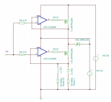
The transistor is inverting with the source to the power and drain to output.
With the Op inverting is its input inverted twice at the output from circuit.
Why did i choose the double inverter?
It is because i dont need 7-10v extra for the transistor gate to get it to conduct full.
The other way around is more common in driving Fets but I choose this way because of no extra PSU for the OP:s. I have a simulation program (TINA from Texas international) that makes it easy for me to get the circuits stable.
The positive slew rate of both circuits should be more than 20 v/us.

that makes sense. What is the reason for the difference between the bipolar driver and the unipolar driver? The bipolar driver has some bias BJTs driving the gate of the FETs, but the second just has opamps driving the gates. If I want to make the second (class-G ish) design bipolar, can I simply add a near identical N-fet section, or do I need to add in the biasing from the first design too?
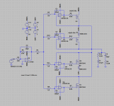
The Mosfets need higher Voltage G to S than bipolar B to E.
On the other hand the mosfets has much lower saturation voltage.
To keep the mosfets advantages it needs a special drive circuit.
But it doesn't have to be more complicated than this.
To observe is that the OP has to be separate for positive or negativ polarity (not included) and rail to rail in and out.
OPA2156 will be great.
Attachments
apologies, maybe I wasnt clear - I meant I would like to make it both source and sink current - with both positive and negative power rails like in comment #15 but also with both low and high power rails like in #22
oh, reading again I see what you are suggesting. I misread.
Yesterday I had the chance to construct a circuit with your suggestion in comment #22. I made the negative side in the same way as the positive side. It seemed to work very well with just the positive IRF9140 side, however when I connected the negative end I noticed some strange heating in the transistors - I didn't manage to find the reason for it before the end of the day, its possible I had something wired slightly incorrectly. I attached a schematic of what I tried to make - does this look like a viable circuit to you?
Now I am playing with the simulation and I notice that while it does work very well, in fact both transistor pairs seem to be on in the low state, which is not what I am looking for - when Vin is below LOW+ only the inner FETs should be on - is there a mistake in my schematic - or your schematic? I notice the outer FET is not actually feeding the inner FET.
The suggestion in #31 makes more sense to me as the outer FET is feeding the inner FET, but in simulation (pictured) it seems not to work that well - the output is clipped and offset (pictured). Have I made some mistake in my layout?
Attachments
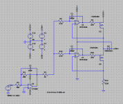
You have a problem with your+ and - high to all fets.
In that way they will deliver 40v to the gate of U3 that is only rated for 20v DS.
And the same for the negativ half. U1 U7 should have negativ feed to ground and U6 +U8 positive feed to ground.
You will also have a problem with max input current to the 2156. The max is 10 mA and it has diodes that conduct when input voltage goes oudside the feed voltages. Thats why i had 4,7k input resistors to the OPs. AS it often goes currnet through the input resistors it is better to take away R1 so the inputs don't affect each other.
Drain of U3 shall not go to output - it should go to source of U9. U3 shall only deliver current when the output is higher than 1v under low+.
And the same for the negativ half.
I would test all fets G-S with an ohmmeter.
It could be a problem with offset voltage or the OP:s but the OPA 2156 are so good i left that thougt. A 10Mohm resistor from input of U7 to negativ low make a dead band of 4,7mv with 4,7kohm in. (crossover distortion)
Good luck.
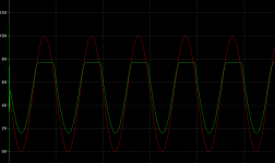
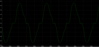
Ive spent a lot of time fiddling around with these circuits and although I've come close, I haven't quite managed to get one which works. The circuit posted in #31 almost work except for a fatal problem - when the opamps are idle, their outputs sit on their positive rail, only when the voltage at the negative terminal is higher than the positive terminal they start to turn on and they take some small amount of time to "find" the operating point of the fet. This isnt that noticeable at audio frequencies but at high frequencies (im testing at 100kHz) this creates a considerable glitch. This also happens at the negative extremity and when the wave crosses 0, which creates a very distorted waveform (pictured). I tried everything I could think of to minimise this, but the switching from one FET to another at high frequency is always problematic.
is there a way to get this to behave?
is there a way to get this to behave?
Attachments
There are always solutions. Sometimes they are hard to find.
I have two suggestions that will make your circuit work better.
You can change to global feedback for U2 = you move R4 from output U2 to R 14.
There is a possibility that C3 must be increased a little bit to avoid self oscillation but it could work just as it is.
Then you can try lower values for R2 and R 10 to make the fets faster. Maybe C1 and C7 can be smaller.
If you still have problems i guess you will need faster OP:s with higher output current to the FETs and maybe an idle current circuit as in audio amplifiers.
- Home
- Design & Build
- Electronic Design
- How to debug class G output stage?