I recently bought a nice embedded digital transport/streaming device (CocktailAudio X10) well knowing that the quality of the DAC and the amp circuitry is fairly poor....
My reason for buying this device anyway is/was that I cannot possibly do better myself than what this device does on the digital side and user interface (ripping CD's to HD, streaming etc.). What I however hope/think to be able to do much better is the DA-conversion and the amplification part of the story🙂
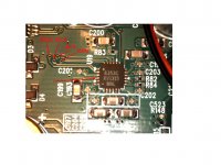
First however I need to tap the I2S signal......
This seems trivial as the DAC chip is easily identifiable and easy to access, however, I find myself in trouble when actually trying to solder on the connecting wires.
I would greatly appreciate ideas/advice on how to do this "tapping" in practice. How do I strip the vias of lacquer preventing me from soldering wires here😕
All advice greatly appreciated,
Nic
My reason for buying this device anyway is/was that I cannot possibly do better myself than what this device does on the digital side and user interface (ripping CD's to HD, streaming etc.). What I however hope/think to be able to do much better is the DA-conversion and the amplification part of the story🙂
First however I need to tap the I2S signal......
This seems trivial as the DAC chip is easily identifiable and easy to access, however, I find myself in trouble when actually trying to solder on the connecting wires.
I would greatly appreciate ideas/advice on how to do this "tapping" in practice. How do I strip the vias of lacquer preventing me from soldering wires here😕
All advice greatly appreciated,
Nic
Attachments
Acetone will remove most PCB conformal coating, I do it at work all the time.
Use a stiff bristle toothbrush and the acetone will clean the coating off.
Use a stiff bristle toothbrush and the acetone will clean the coating off.
Its not conformal coated though.
You could just use a scalpel, and carefully scrape the coating off the vias, or solder directly to the chip pads/leads, or, trace where the vias lead to on the other side of the board, as they may connect to larger pads/components that you can more easily solder to 😉
You could just use a scalpel, and carefully scrape the coating off the vias, or solder directly to the chip pads/leads, or, trace where the vias lead to on the other side of the board, as they may connect to larger pads/components that you can more easily solder to 😉
The via through the board is not coated so as long as you can find a wire that fits through it would solder to the via itself and make a good joint anyway.
Thanks for the advice.
Finding the right wire is indeed also a problem as the vias are indeed very narrow. I was thinking to use something stronger and stiffer than copper. Just don't know what.
Unfortunately no "big" components on the signal path and also the pads of DAC chip are tiny. I still think the vias should be the easiest place to connect.
Thanks for the advice.
Finding the right wire is indeed also a problem as the vias are indeed very narrow. I was thinking to use something stronger and stiffer than copper. Just don't know what.
Unfortunately no "big" components on the signal path and also the pads of DAC chip are tiny. I still think the vias should be the easiest place to connect.
Take an old computer cable (printer, com port) and remove 1 lead. Strip the insulation and remove 1 strand from the wire. I use those to repair acid damage on old (early '90s) broadcast gear PCBs . You shouldn't need 'strength' just a reliable connection. I've used this wire to 'splint' smaller than 8 mil tracks.
I use a razor blade or exacto knife to remove the coating (usually green) by gently scraping it. A flux pen simplifies soldering to the tiny traces. when the strand is soldered in an both ends the razor blade or exacto will cut the excess strand and not damage the printed trace. It's tedious but is almost invisible when done.
G²
Not recommended, the solder resist used on PCBs is usually an epoxy, of a similar type as that used in the FR4 that makes up your PCB, if you can attack the solder mask it will attack the FR4, not good.
The way it is done is by using one of these or a similar abrasive device...
Abrasive Fibreglass Pencil | Maplin
The way it is done is by using one of these or a similar abrasive device...
Abrasive Fibreglass Pencil | Maplin
Look for wirewrap jumpers.
Like this:
search for " PAGE, Wire Wrap, 30 AWG 9" Pre-Cut & Pre-Stripped Wire w/ 1" Blue Insulation "
on e-bay.
(some links to ebay don't work well so this is easier)
Like this:
search for " PAGE, Wire Wrap, 30 AWG 9" Pre-Cut & Pre-Stripped Wire w/ 1" Blue Insulation "
on e-bay.
(some links to ebay don't work well so this is easier)
Dichloroethylene was recommended by TI in their service manual for DFS V.
I never used it for lack of opportunity.
Gajanan Phadte
I never used it for lack of opportunity.
Gajanan Phadte
Dichloroethylene was recommended by TI in their service manual for DFS V.
I never used it for lack of opportunity.
Gajanan Phadte
MSDS here:
https://www.mathesongas.com/pdfs/msds/MAT23670.pdf
Not on my list of stuff to buy.
🙂
- Status
- Not open for further replies.
- Home
- Design & Build
- Construction Tips
- How to "clean up" a tiny via for soldering?