Sorry, my friend (MerlinB) … I'm confusing nothing of the sort.
gm = μ / Rp for vacuum tubes (biased into conduction)
gm = Id / Vgs for FETs (biased into conduction)
gm = Ic / Vtherm for BJTs? But
Ic = hFE·Ib and Vtherm is a constant for some specified material (silicon) and temperature (nominal 300°K) so…
gm = hFE Ib / C and since
Ib ≡ K e((VBE - Vthr) / kT ) … we then have
gm = hFE K e((VBE - Vthr) / kT )
which unlike either the vacuum tube, or FET is hugely nonlinear with VBE voltage. Gigantically. Ridiculously.
Contrary to that, AV (voltage gain) of a BJT for grounded-emitter (or capacitor-bypassed emitter self-bias resistor) is nearly a linear product of:
AV = hFE RC / Zin.
Where Zin is the Thevenin equivalent impedance of the Vcc voltage divider and any series resistance from input to base/bias node. That part is quite linear. Note that gM just doesn't really figure into it.
Its also really grating for people to call "hFE a defect". It is one of the only linear characteristics of bipolar transistors that "tames" the otherwise hideously exponential behavior of an ordinary PN junction.
Peace, bro.
GoatGuy
Of course it doesn't figure into it- you deliberately ironed it out in the algebra! You can of course re-write it as:AV = hFE RC / Zin.
Note that gM just doesn't really figure into it.
AV = gmRC * VT/(IBZin)
This makes it more obvious that you have a transconductance device which produces an ideal gain of gmRC, but this is 'dragged down' by the defect of base current, i.e. hFE.
Compare this with a valve, for example:
AV = gmRa * ra/(ra+Ra)
here again you have a transconductance device which produces an ideal gain of gmRa, but this is 'dragged down' by the defect of the valve's internal resistance ra.
The exponential nature of the device is just another defect, but does not change the fact that it is Vbe which controls Ic. Take any BJT, operate it at 1mA and you will always have a gm of 40mA/V. Apply the same dVbe and you will always get the same dIc. Only the base current necessary to bias the device 'on' will be different among the different devices. This universal consistency of gm between different devices ought to be an obvious clue that it is the fundamental govening feature of BJTs! It is also why the hybrid-pi model is so prevalent:Its also really grating for people to call "hFE a defect". It is one of the only linear characteristics of bipolar transistors that "tames" the otherwise hideously exponential behavior of an ordinary PN junction.
Last edited:
When people first learn about BJTs they are told about beta, and get the idea that BJTs are a current-driven device - but with a gain which is almost random from one sample to another. Later, hopefully, they learn about Ebers-Moll and realise that gm is highly predictable and is the key to designing precision circuits. Many get stuck at the first stage.
The BJT is hugely non-linear, but reliably and predictably so. Hence we can use circuits like LTP, or add emitter degeneration, and calculate precisely how the circuit will behave. You can't do that for a 'beta-derived' circuit - you would need to do a Monte-Carlo parameter spread analysis for every circuit.
The BJT is hugely non-linear, but reliably and predictably so. Hence we can use circuits like LTP, or add emitter degeneration, and calculate precisely how the circuit will behave. You can't do that for a 'beta-derived' circuit - you would need to do a Monte-Carlo parameter spread analysis for every circuit.
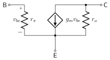
So, looking at the hybrid-pi model above. If I have an arbitrary BJT and apply a voltage to B (say 200V) how much current will flow from E to C when the BJT is configured as a voltage follower (NPN common collector)? What data sheet parameters can I use to figure this out? Does the normal operation of a voltage follower involve a saturated base, or is it kept out of saturation somehow?
What happens if there is nothing downstream to draw that much current? Does the voltage sag or do fewer electrons flow?
What happens if there is nothing downstream to draw that much current? Does the voltage sag or do fewer electrons flow?
Put the base at 200V. Put a resistor from emitter to ground. The current through the resistor is given by Ohm's Law: (200-0.6)/R. The 0.6 is approximate, but close enough. How much of this emitter current ends up in the collector depends on collector voltage. If it is 200V or above then almost all of it will go to the collector. If a bit below 200V then all of it will come from the base. If any lower than this then the collector-base junction will become forward biased and will try to drag down the base voltage.
The hybrid-pi model is a small-signal model, i.e. it only works for small AC signals, not DC.So, looking at the hybrid-pi model above. If I have an arbitrary BJT and apply a voltage to B (say 200V) how much current will flow from E to C
To answer your question, it depends on the voltage you apply between base and ground, and what emitter resistor you choose. It also depends on hFE, though only to a small extent if hFE is large.
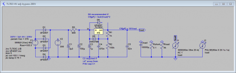
After all this bjt theoretics please have a look at the attached regulator. I modified my proposal using the TL783 a little and double checked all kind of operating and fault conditions.
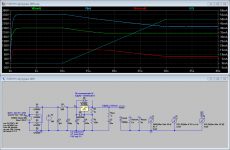
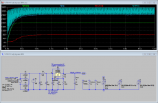
It puts out ~200V at constant 50mA with NO measurable ripple (thanks to the voltage dropping CRC pre-filter). The output impedance is <0.1 ohm within the audio range. Mains voltage may vary by up to +/-10% from nominal with regulation maintained.
I was not able to exceed the SOAR under any conditions. You can start up into constant current load, resistive or capacitive or mixed, into a short or open circuit... Same goes for power down, whether you have big capacitance in the downstream circuit discharging into the psu or not, whether the circuits shorts or drops out, or mains power removed any time.
The TL783 needs a chunky heatsink, but so would any design using a power bjt in its place.
Attachments

So, let's say that Vin is 200V, from a well-regulated supply that can sink infinite current. Let's also say that V+ is 300V, from a similar supply. And further, the load on Vout is about 20mA, i.e. Re about 10K.
I accept that V+ is going to be 200 - junction voltage (0.6 or whatever for a silicon BJT).
What I don't understand is how to choose a transistor that works in this application. How much current gain is happening in the scenario I just described? If the BJT has a beta of 1, does that mean that there is a draw of 20mA through the base, and if it has a beta of 2, then there is a 10mA draw through the base, and so on?
This seems to me like a backwards way of thinking about gain? In an op-amp circuit, the gain is constant and the output is the input times the gain, provided the rail voltage is high enough.
But if this way of thinking holds, then, I could pick a transisitor with a beta of 200 and be confident about a 20mA output, so long as the base can source 20/200mA of current without sagging? And provided the max power dissipation and Vbe of the part are not exceeded, of course.
So, then, how to know if the transistor has a beta of 200 [or more] under these conditions? We go to the datasheet and look at the beta (hFE) graph. Then we analyze a couple of other values (corner/edge cases of our requirements) and see if they also work?
Is this the Monte Carlo approach you mentioned? It seems picking a transistor for even a simple application is tricky these days!
Wes
Thanks, Goldenbeers. That circuit is a bit more familiar to my experience level, I used to float 78xx regulators to make variable power supplies in days of yore.
Looking at the TL783 circuit, we can have a maximum Vin of 353-X, where X is the voltage drop of R3. The TL783 has an absolute max rating of Vin-Vout = 125V, so we need X to be at least 228V.
To get a voltage drop of 228V across a 680 ohm resistor, we need to draw 335mA of current. The works back to a 77VA draw just to keep the TL783 within its ratings, exceeding the power rating of my transformer by 52VA.
Obviously I'm missing something here.....any ideas what?
Obviously I'm missing something here.....any ideas what?
You already said it, the max Vin-Vout is 125V, NOT the max Vin.
Vout will be 200V, so max Vin under steady conditions is 325V. Not 125V.
The trick is to lay out the schematic such that during power up / down, when either Vin or Vout will be/go to 0V at some time, the 125V max differential voltage is never exceeded. Same for most or all conceivable fault conditiond like shorts or open circuits before or after the regulator, at any time.
The TL783 ha some built in protections, other conditions can be made safe by using diodes or zeners or other similar stuff.
The art is achieving all this in a safe manner with a minimum number of parts and no excessive heat burn off.
IIUC, the VPS230-115 transformer doubles the incoming line voltage when the secondaries are wired in series. Line voltage of 125Vrms is possible (and not uncommon) here. This means that 250Vrms is possible on the secondaries of the transformer. 250 * 1.4142 = 353.550. The forward voltage drop for a UF4007 is 1.7V, so the test point V2 can see 351.85V. With only the load from R1+R2 (1.35mA) the voltage drop at R3 is only 0.9V, putting the no-load input on the TL783 at a theoretical maximum of 351 - if Vout is 200V, then the differential voltage is 151V. Have I missed something here?
Yes.wes-ninja250 said:But if this way of thinking holds, then, I could pick a transisitor with a beta of 200 and be confident about a 20mA output, so long as the base can source 20/200mA of current without sagging? And provided the max power dissipation and Vbe of the part are not exceeded, of course.
No. The Monte-Carlo approach is to pick random values for relevant parameters (e.g. beta) and calculate what the outcome is. Repeat many times. If most of the outcomes are satisfactory, then the design is satisfactory. The alternative is to do a full sensitivity analysis, which may be more work - especially if there are a number of relevant parameters which interact in non-intuitive ways.Is this the Monte Carlo approach you mentioned?
With only the load from R1+R2 (1.35mA) the voltage drop at R3 is only 0.9V, putting the no-load input on the TL783 at a theoretical maximum of 351 - if Vout is 200V, then the differential voltage is 151V. Have I missed something here?
Yes. Under 15mA the TL783 drops out of regulation. Just a little current will trickle thru. The zener D5 (a 100V type) will protect the TL783 max differential voltage between in&out terminals to about 100V (actually less). All the minimal trickle current will be shunted to ground thru R2.
Edit: Yes, it also means that Vout will be >200V if no current (<15mA) is drawn from the circuit. If you don't like it, you could lower R1,R2 so that sufficient current will be drawn at any time, but this wastes a lot of power during normal operation, so better avoid this if you can.
Last edited:
Man, I really to need to learn how to use some of these simulation tools. I used to have a package for Windows that was easy to use, but I no longer use Windows.
What I don't understand is how Vin-Vout stays under 125V when load is 50mA. By my calculations, at max mains voltage (yielding 250Vrms on the transformer's secondary winding), R3 would need to drop at least 28V.
What I don't understand is how Vin-Vout stays under 125V when load is 50mA. By my calculations, at max mains voltage (yielding 250Vrms on the transformer's secondary winding), R3 would need to drop at least 28V.
Member
Joined 2009
Paid Member
I used to have a package for Windows that was easy to use, but I no longer use Windows.
I believe spice is available on many platoforms. LTspice is available for PC under Windows and iMac OSX (although the interface sucks).
Have a look at the attached diagram.
V002 is the voltage after the rectifier. It will indeed go up to 360V, but peak!
The small valued C1 will drop this to 317V mean, with 50mA load, which becomes ~281V after R3. No probs for the TL783 to drop the 81V down to 200V at the output.
As a nice side effect, the small C1 will result in benign charge peaks, reducing noise interference thrown back into the power tranny.
Attachments
Member
Joined 2009
Paid Member
Is it possible that when the mains AC is running a little high and that 50mA load hasn't started to pull current - the voltage may swing higher a turn-on ?
See diagram in #74 🙂
Should be no harm for classic tube circuits, as they all can take some excess voltage over quiescent state as long as little current is flowing (and hence, little power dissipated)
Could be problematic if you have SS pieces downstream relying on B+ never exceeding the spec value.
Should be no harm for classic tube circuits, as they all can take some excess voltage over quiescent state as long as little current is flowing (and hence, little power dissipated)
Could be problematic if you have SS pieces downstream relying on B+ never exceeding the spec value.
This is very interesting. I never considered that idea that it was possible to lower the (average) voltage before the regulator by using an initial capacitor that was too small for the DC to achieve its full potential.
Is the value selected for 50 or 60Hz AC mains?
Is the value selected for 50 or 60Hz AC mains?
- Status
- Not open for further replies.
- Home
- Amplifiers
- Tubes / Valves
- How little B+ ripple do I really need?