abraxalito: I had wondered about doing this with a souncard. I have an old M-audio usb audio interface that might make a good candidate.
N101N: I'm really not confident with discrete transistor design, not my area of expertise at all. Grounded base, in particular, does my head in 🙁 Much happier with opamps
After further reading today, current thinking is an lme49721 based ItoV followed by probably some lme49720 based active filters.
ultimately the whole system is actively crossed 2 way anyway (FWIW ESP 101 power amps and lme49720 based LR 24db crossover) so there's no avoiding the opamps
For design 2, I don't understand the bias circuit. It looks like you make a current that depends on the difference between the base-emitter voltages of D1 and Q1, but since these are unequal devices, I would expect it to spread a lot. More importantly, I don't understand why you need this current in the first place.
D1 is a LM329 Zener reference. The BJT symbol is just an effect of my schematic software and the LM329 TO-92 package (sorry). The 2mA compensation current is necessary to force the output of the TDA1541A to near zero mV as the compliance voltage of the DAC is very low (+/-25mV) and it has a unipolar 0 to -4mA output - digital zero is at -2mA. This current source works extremely well and was tuned to be accurate to approximately 5-6 digits (2.0000mA), keeping the output compliance of the DAC well within its needed range.
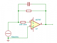
This is also why you wouldn't want to use the 100 ohm resistor in series with the inverting input (outside of the feedback loop) as it would cause an offset voltage to appear on the DAC output instead of the near-perfect virtual ground provided by direct connection to the inverting input.
Page 14 of the same datasheet says that if CL is greater than 33pF, then the 100ohm ESR is required. Since it's 2.2nF for the TDA1541, this is absolutely necessary in this position.
Last edited:
OK, design 2 makes sense now!
Regarding the 100 ohm and design 1, what I meant is to connect it between the node where the feedback network is connected to the DAC and the negative op-amp input. That is, only the current through the op-amp's negative input would cause voltage drop across this resistor, the DAC current would flow straight into the feedback network.
Regarding the 100 ohm and design 1, what I meant is to connect it between the node where the feedback network is connected to the DAC and the negative op-amp input. That is, only the current through the op-amp's negative input would cause voltage drop across this resistor, the DAC current would flow straight into the feedback network.
Attachments
Last edited: