Hi millwod, I think you may have missunderstood me there, I was just asking because mbh's power dissipation values were way above anyhting I had ever contemplated for this design, so I was just wondering how he had done it, not how to do it in general.
If you haven't found any end-mounting resistors yet, check out CPC part RE01296 is an example.
Also check out their part CA01882 for an example 5mm pitch electrolytic cap.
I have found the caps other people are recommending on here to be very hard to get hold of in UK. I suggest you check out the Sanyo 2SA1016/2SC2362 pair from Profusion
Happy building, I am almost ready to build my own modified P3A with my own PCB 🙂
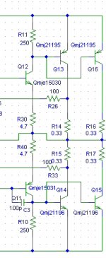
Thought I would add a quick note about how I am sharing output devices in a high power p3a amp I am working on (again after at least a year of not touching the thing). This method is fairly common among Randy Slone's toplogies and seems to work well. At 200W into 4 ohms, each device dissapates about 65-70W according to PSpice with 56V rails.
You can disregard R26 and R33, they are just reference for a protection circuit.
You can disregard R26 and R33, they are just reference for a protection circuit.
Attachments
Can some one tell me if is correct and will work to substitute the output stage (mje) with 2sa1516/2sc2922?
by this way? Did u or someone tested in this configuration?
An externally hosted image should be here but it was not working when we last tested it.
MaXiZ, the sch you show is from the P3 project.
In the P3A the results may be sactisfatory...
See this:
Must change MJL4302 to 2SA1516 and MJL4281 to 2SC2922
(if the img doesn't appear, right-click and 'show image')
Also check this thread as I answered to your question yesterday. There is some explanation on using those 2SA and 2SC
In the P3A the results may be sactisfatory...
See this:
Must change MJL4302 to 2SA1516 and MJL4281 to 2SC2922
An externally hosted image should be here but it was not working when we last tested it.
(if the img doesn't appear, right-click and 'show image')
Also check this thread as I answered to your question yesterday. There is some explanation on using those 2SA and 2SC
oh ok.. sorry... and do u know a good alternative to mje/mjl? Here in italy they're so expensive..
Must change MJL4302 to 2SA1516 and MJL4281 to 2SC2922
The 2SA1216 is the complementary to 2SC2922.. Not the 2SA1516.
/Freddie
Excuse me again but the datasheet say that the MJ4302/MJL4281 are 250W... why Rod write 60-100W???
MaXiZ,
The power rating of the transistor and the amplifier are only loosely related, and the max power dissipation of the transistor is much, much bigger than the power of the amplifier in which it is used.
A bipolar transistor is often destroyed in an audio amplifier by a process called 'secondary breakdown'.
This means that as the voltage across the device, between collector and emitter, increases, then the current through the device is limited by this phenomenon.
A 2SC2922, for example, is rated at 200W. Using a 10mS pulse, a good indication of an audio signal in a Class AB amplifier, the secondary breakdown figures are:
35A of collector current at 20V between collector and emitter
10A of collector current at 60V between collector and emitter
1A of collector current at 180V between collector and emitter
You will notice how sharply the collector current drops with increasing voltage. Instantaneous dissipation at 35A/20V is no less than 700W, at 10A/60V it is 600W, yet at 1A/180V it is just 180W!! This is clearly a very important limitation, and in fact is a major source of failure in audio amplifiers.
A complicating factor is the reactive load of a loudspeaker. This distorts the normal relationships between applied current and voltage, and can see very high voltages across devices while passing appreciable current. When this happens, devices fail regularly if the design does not account for it.
Fortunately, if the rails are say 40V, and the transistor has 30V across it, then the load must have only 10V across it, so is passing low current, no more than a couple of amps. So, this looks fine, although the reactive kickback of the speaker is not accounted for here and things are usually worse than they seem.
The result of all this is that we must design for secondary breakdown with bipolar transistors, and a higher rail voltage is often a dangerous design decision. We normally get around this problem by using multiple pairs of devices, so the current is spread across number of transistors, reducing the change of secondary breakdown.
Ciao,
Hugh
And we sometimes tend not to run the output near it's full rating...to get longer life?? I guessing MAxiZ needs about 250W?? Go try the M250 here.http://www.astro.uu.se/~marcus/private/m250.html
"Excuse me again but the datasheet say that the MJ4302/MJL4281 are 250W... why Rod write 60-100W???"
Semiconductor ratings take some study to understand.
The forward bias safe area of operation at 25*C for the MJL4302/4281 is 100W at 100V. That is for 1 second, and is non-repetitive. I am going to ignore this here because of the lower voltage involved. In a 400W amp this would be vital.
For temperatures higher than 25*C the device must be de-rated. For plastic devices the maximum junction temperature is 150*C, for metal cased TO3 devices, 200*C. At 100*C junction temperature the plasic part can handle about 40% of its maximum power, the metal part can handle about 60%. The thermal resistance from junction to case on the MLJ part is 0.54*C/W. If we assume the amplifier could be mounted in a glass front rack (typical hi-fi), the ambient air can reach 55*C. If we have a big heatsink it will have about 1*C/W resistance. Semiconductor mounting can be from about 0.3*C/W~0.6*C/W, depends on case style and insulator type. Subtract 55* from 100* and you have 45* to work with. Add 1* + 0.46* + 0.54* and you get 2*. In a real rack, with real heatsinks, with real mounting, 22.5W will cause a junction temperaure of 100*C (water boils). Increasing the power another 25W to 47.5W will hit the maximum junction temperature. The metal part can take about 50% more power before hitting its maximum.
How long will a part run at maximum?
Not very long.
Every 10*C you can lower the temperature will generally double the life span.
A rule-of-thumb: metal parts can handle 1/6 of their 25*C rating with typical heatsink/mounting/ambient, plastic about 1/9 of their 25*C rating. Call it 40W for MJ21193/94 and 25W for MJL4302/4281.
A moderate bias class AB amplifiers with unregulated supply is about 60% efficent, so a 100W amplifier can have about 40W worth of heat to get rid of, a 60W amplifier about 25W. You have two outputs, but that is not twice as much power. A 50% duty cycle only increases power handling by about 1.414, and this quickly goes away when driving a reactive load (a real loudspeaker may be 45*). This helps explain why the ESP3A with a pair of MJ21193/94 is only pushed to 100W and the AKSA to 55W with plastic.
Speed.
While this pair is fast at low current, 50Mhz at 1A, the speed drops like a rock at higher collector current, about 3Mhz at 5A. This is typical for this kind of part.
At 5A the MJ21193/94 are just as fast.
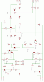
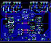
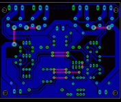
Hi, after a bit of a hectic weekend moving from one end of the country to the other, I have finaly finished teh second revision of my high power P3A design, so I thought I would post teh revised scematics and board layouts so people can look for more mistake or give me some more pointers.
First up is the ne schematic, which has teh correctly paralled output devices, allong with the correct small signal transistors that I intend to use. I have also included a resistor at the base of T7 to try and keep things a little more stable as the gain devices will be running under a little more stress than normal.
First up is the ne schematic, which has teh correctly paralled output devices, allong with the correct small signal transistors that I intend to use. I have also included a resistor at the base of T7 to try and keep things a little more stable as the gain devices will be running under a little more stress than normal.
Attachments
Freddie said:
The 2SA1216 is the complementary to 2SC2922.. Not the 2SA1516.
/Freddie
😀 😀
That's right... Just look to the right side of your keyboard: the 5 is upon the 2 key... That's the result of fast key pressing... 😉
ttt.
I got my MJL4203 and 4281a devices, still waiting on mje15035/15034s to arrive . I am shooting for 100 watt per channel at 8 ohm, stable down to 4 ohm loads
I got my MJL4203 and 4281a devices, still waiting on mje15035/15034s to arrive . I am shooting for 100 watt per channel at 8 ohm, stable down to 4 ohm loads
- Status
- Not open for further replies.
- Home
- Amplifiers
- Solid State
- High Power P3A design questions.