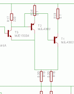
Hi, I'm not too sure why it's there, but it looks like it will be acting as a fairly large miller capacitance for that driver. I guess it could be being used to try and balance the response of the two diferent PNP and NPN output devices, but I have no real idea what it does I just included it because it was there in Rod's design.
If I get bored over the holiday and fancy a bit more pracitce ofr my RF amplifier course here I may take a closer look at it and see what effect it has on teh frequency response of the amp as a whole.
If I get bored over the holiday and fancy a bit more pracitce ofr my RF amplifier course here I may take a closer look at it and see what effect it has on teh frequency response of the amp as a whole.
bigparsnip said:Hi, I'm not too sure why it's there, but it looks like it will be acting as a fairly large miller capacitance for that driver. I guess it could be being used to try and balance the response of the two diferent PNP and NPN output devices, but I have no real idea what it does I just included it because it was there in Rod's design.
If I get bored over the holiday and fancy a bit more pracitce ofr my RF amplifier course here I may take a closer look at it and see what effect it has on teh frequency response of the amp as a whole.
Well, the miller effect depends on voltage gain at that point of
the circuit, so it won't be multiplied much ? the same capacitor
is present in the now defunct P3 design - I checked.
From reading my PA design book by D.Self I can't work out
why its there, but the rest of the circuit makes sense.
🙂 sreten.
Re: Re: HO P3A
Hi, I must have missed this post earlier, not too sure how, but it didn't seem to appear for a bit untill after some of the others.
Anyway, do you ahve a link to a data sheet for the above devices? I did a quick google search, but the only one I found was in Japaneese I think.
Also, as far as the parts go, I wasn't going to go quite as far as blackgates, to me they just seem a littel too pricy (I'm only a student), but I had trouble finding suitably sized 100uF n/p caps (all the ones I found were quite large and made the PCB rather awquard to design in eagle). However, if people could point out some decent 100uF caps that will fit into the 5mm pitch of the board I would be interested to know about them (allong with the verticaly mounting output resistors).
mhb said:Regarding your circuit, use Toshiba 2SC1775As for the differential pair, trust me on this, the sound improvement is not slight. They are rated >100v. The pin config is different from most, so double-check your board. Also you MUST match the pair as the 1775's gain varies
Hi, I must have missed this post earlier, not too sure how, but it didn't seem to appear for a bit untill after some of the others.
Anyway, do you ahve a link to a data sheet for the above devices? I did a quick google search, but the only one I found was in Japaneese I think.
Also, as far as the parts go, I wasn't going to go quite as far as blackgates, to me they just seem a littel too pricy (I'm only a student), but I had trouble finding suitably sized 100uF n/p caps (all the ones I found were quite large and made the PCB rather awquard to design in eagle). However, if people could point out some decent 100uF caps that will fit into the 5mm pitch of the board I would be interested to know about them (allong with the verticaly mounting output resistors).
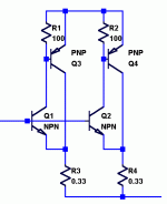
I think you should have emitter resistors for the parallel outputdevices and the collectors should be connected together.
Best regards
Selim
The resistors are in the correct position
for a CFP (complementary follower pair), but
What is wrong is the two paralelled output devices should share
the same resistor, the collectors should be connected together,
as you say. The resistor value needs to be halved.
🙂 sreten.
better output Q current sharing requires either:
emitter resistors for each output device
or doubling dirvers to put both output Qs inside separate CFP loops with the two present resistors in the "emitters" of the two paralleled CFP
also you need to read up on 2nd breakdown in bipolar devices, you can't always safely use even 1/2 the rated Vce when devices begin to seriously heat up, driver Qs can easily fry from undersizing
also large distortion can result from inadequate current gain, look at min Hfe for the output pairs and see if the VAS bias current is high enough; maybe add a emitter follower stage
just add that adding emitter resistors as Selim suggests
would help in ensuring current sharing, but from the designs
I've seen presumably the internal resistances of the transistors
are enough to keep things under control.
🙂 sreten.
would help in ensuring current sharing, but from the designs
I've seen presumably the internal resistances of the transistors
are enough to keep things under control.
🙂 sreten.
Re: Re: Re: I'm mystified why C7 (100pF) is there ?
Do you mean C5 not C4?sreten said:
Nope, C4 (100pF) is the miller compensation capacitor.
🙂 sreten.
Re: Re: Re: Re: I'm mystified why C7 (100pF) is there ?
your quite right, it is C5 (100pF) not C4.
🙂 sreten.
markp said:
Do you mean C5 not C4?
your quite right, it is C5 (100pF) not C4.
🙂 sreten.
jcx said:better output Q current sharing requires either:
emitter resistors for each output device
or doubling dirvers to put both output Qs inside separate CFP loops with the two present resistors in the "emitters" of the two paralleled CFP
So, if I conect both collectors to R19 (or R27) and then include seperate emitor resistors for each device, it would give better control over q curent and still alow decent current sharing between the two devices?
also you need to read up on 2nd breakdown in bipolar devices, you can't always safely use even 1/2 the rated Vce when devices begin to seriously heat up, driver Qs can easily fry from undersizing
At the rail voltages I intend on using (up to +/- 50V) the devices are good for up to 4 amps each, which would give enough headroom for about 250w into a four ohm load, which agian is about what I would be aiming for as a maximum for this design.
also large distortion can result from inadequate current gain, look at min Hfe for the output pairs and see if the VAS bias current is high enough; maybe add a emitter follower stage
Right, going fromt he data sheet, it looks as though the gain should stay abouve 100 for the currents I should be running through the output. And, as the drivers for these are fairly beefy in themselfs (max Iout of 4A) I don't think that this will be a problem here.
Right, so taking into account what was said above, do people think that the arrangement below is how I should be going with the design (I have only kept the two resistors at the colectors to keep the board layout simmilar, and allow the use of two lower power resistors in place of one large one)?
It does make a lot more sense to keep things this way, as both output devices are now int eh local feedback loop of the driver, and they should still be able to share current between themselfs.
Andrew.
It does make a lot more sense to keep things this way, as both output devices are now int eh local feedback loop of the driver, and they should still be able to share current between themselfs.
Andrew.
Attachments
250w
Parsnip,
The maximum safe output for your Onsemi output transistors is:
@120 deg farenheit - 186 watts
@130 deg 176
@140 166
At 50v I think you will have difficulty keeping the tranny temperatures below 120 unless you use fans. You can see that every 10 degrees in excess of 68 deg farenheit reduces the maximum power output by roughly 10 watts. Also you'll find the quiescent current hard to stabilize without some cooling for the drivers.
So at 130 degrees (55c) and 4 ohms, you'd be exceeding Onsemi's recommended operating area at anything greater than roughly 42v.
Better safe than deaf,
M
hifi said:that if you dont care to match them 🙂
/ micke
Pardon?
You mean this is the way to do it if I don't want to match them, but if they were to be closely matched, they wouldn't need the emiter resistors?
they would still need the emitter resistor. but they wouldnt need to share it,
they are shared to forcefully share the current between the devices,
/ micke
they are shared to forcefully share the current between the devices,
/ micke
Re: I'm mystified why C7 (100pF) is there ?
I contacted the designer and its to prevent parasitic oscillation.
The new scheme with the 0.33R resistors paralelled is correct.
Note bias current will be double that of the single pair output.
In D. Self's design the emitter resistors are omitted.
In fact his "Load Invariant Design" using a parallel CPF pair
is more advanced in most respects than Rod's P3A design.
🙂
sreten said:What is its purpose ?
can some-one elucidate me ?
🙂 sreten.
I contacted the designer and its to prevent parasitic oscillation.
The new scheme with the 0.33R resistors paralelled is correct.
Note bias current will be double that of the single pair output.
In D. Self's design the emitter resistors are omitted.
In fact his "Load Invariant Design" using a parallel CPF pair
is more advanced in most respects than Rod's P3A design.
🙂
Re: 250w
I understand what you are saying about the derating of the devices, but how have you worked out how much power each device will be dissipating?
Assuming the worst, say the amplifer is only 50% efficient at full load into 4 ohms (which it shouldn't be, as it should be capable of >60% efficiency), the total dissipation in the four output transistors would be 250 in total. This only works out to be around 60W per device which they should be able to handle without any problems at all.
mhb said:Parsnip,
The maximum safe output for your Onsemi output transistors is:
@120 deg farenheit - 186 watts
@130 deg 176
@140 166
At 50v I think you will have difficulty keeping the tranny temperatures below 120 unless you use fans. You can see that every 10 degrees in excess of 68 deg farenheit reduces the maximum power output by roughly 10 watts. Also you'll find the quiescent current hard to stabilize without some cooling for the drivers.
So at 130 degrees (55c) and 4 ohms, you'd be exceeding Onsemi's recommended operating area at anything greater than roughly 42v.
Better safe than deaf,
M
I understand what you are saying about the derating of the devices, but how have you worked out how much power each device will be dissipating?
Assuming the worst, say the amplifer is only 50% efficient at full load into 4 ohms (which it shouldn't be, as it should be capable of >60% efficiency), the total dissipation in the four output transistors would be 250 in total. This only works out to be around 60W per device which they should be able to handle without any problems at all.
re: parallel
Pars,
Yea, forgot you added output trannies. Watch the drivers, though, they will get quite hot. And that'll increase quiescent current which will add to thermal stress of the outputs.
M
Pars,
Yea, forgot you added output trannies. Watch the drivers, though, they will get quite hot. And that'll increase quiescent current which will add to thermal stress of the outputs.
M
Re: Re: 250w
some simulation packages do that for you (protel dxp for example). Short of that, you can manually calculate it.
bigparsnip said:but how have you worked out how much power each device will be dissipating?
some simulation packages do that for you (protel dxp for example). Short of that, you can manually calculate it.
- Status
- Not open for further replies.
- Home
- Amplifiers
- Solid State
- High Power P3A design questions.