Hi All, I need some guidance.
I am working on a Hifonics Hercules VIII and it has me completely beaten.
I cannot figure out why the power supply will not start up.
Some background:
Once the LM324 was re-installed the amp would not work, once again. I reinstalled it, thinking that the muting circuit was not being disabled and wanted to test the audio.
I can see that the TL594 is not working due to Pin1 being > than Pin2, but I cannot find the source for the voltage I am measuring on Pin1. I have confirmed that the TL594 has the saw tooth wave form on pin 5 as expected and the regulator seem to be working fine. As mentioned before, when I pull Pin3 low, it seem to work (even though not in a regulated configuration)
For reference here are the voltages on the TL594:
1) 8.200 V
2) 4.947 V
3) 4.846 V
4) 0.750 V
5) 1.462 V
6) 3.512 V
7) 0.001 V
8) 11.90 V (that was supply voltage at the time of measuring)
9) 0.000 V
10) 0.000 V
11) 11.90 V
12) 11.16 V
13) 4.977 V
14) 4.977 V
15) 10.14 V
16) 5.570 V
Any advice would be great!
I am working on a Hifonics Hercules VIII and it has me completely beaten.
I cannot figure out why the power supply will not start up.
Some background:
- Amp came in completely dead.
- There are no shorted outputs or drivers to the outputs
- It is a class A or A/B amp as far as I can tell
- The power supply MOSFETs are operational. I can verify that it works as designed by pulling Pin3 of the TL594 low.
- It is a regulated power supply with a voltage divider between V+ and GND going to Pin1 and V- to Regulated 5V going to pin 2.
- I had the LM324 removed from the driver and once observed the power supply working as designed, beutifully
- The LM324 was tested outside of the circuit in a breadboard and functioned the way I expected.
- The protection circuit seems to work different than most amps as it seems like it pulls Pin15 down, rather than pulling pin16 up as I am used to seeing.
Once the LM324 was re-installed the amp would not work, once again. I reinstalled it, thinking that the muting circuit was not being disabled and wanted to test the audio.
I can see that the TL594 is not working due to Pin1 being > than Pin2, but I cannot find the source for the voltage I am measuring on Pin1. I have confirmed that the TL594 has the saw tooth wave form on pin 5 as expected and the regulator seem to be working fine. As mentioned before, when I pull Pin3 low, it seem to work (even though not in a regulated configuration)
For reference here are the voltages on the TL594:
1) 8.200 V
2) 4.947 V
3) 4.846 V
4) 0.750 V
5) 1.462 V
6) 3.512 V
7) 0.001 V
8) 11.90 V (that was supply voltage at the time of measuring)
9) 0.000 V
10) 0.000 V
11) 11.90 V
12) 11.16 V
13) 4.977 V
14) 4.977 V
15) 10.14 V
16) 5.570 V
Any advice would be great!
Attachments
Yes, Pin1 is causing the 594 to shut down. Should I replace the 594, since I cannot see any voltage source that would drive it to 8.2V I am measuring?
Here is a partial diagram of the Power Supply breakout board. It is not complete and may still have errors in it.
Pin1 on the board goes through a 43K to +47V and Pin 2 Goes to a divider formed between Ref (+5V) 2K2 and 43K to -47V.
I measure 8.2V on pin 1 of the 594 and only 4.954 V on the +47V side of the 43K resistor. It looks as if pin1 of the 594 is sourcing the voltage 😕
Pin1 on the board goes through a 43K to +47V and Pin 2 Goes to a divider formed between Ref (+5V) 2K2 and 43K to -47V.
I measure 8.2V on pin 1 of the 594 and only 4.954 V on the +47V side of the 43K resistor. It looks as if pin1 of the 594 is sourcing the voltage 😕
Attachments
How are the 594 voltages different when the amp is functioning as it was when you read the rail voltage?
When the power supply was working correctly both pin 1 and 2 on the 594 was around 2.600 and 2.599 respectively. This only happened once and the LM324 was out of the circuit at that time.
I will go look at the voltages on the LM324 now and report back, but I could not find a connection between the LM324 and Pin1 on the 594.
I will go look at the voltages on the LM324 now and report back, but I could not find a connection between the LM324 and Pin1 on the 594.
That's what is supposed to be. The positive rail pulls pin 1 up and the negative rail pulls pin 2 down and when the two match, the power supply knows that the target rail voltage has been met and the duty cycle is rolled back. When pin 1 is so high, the 594 is being told that the rail voltage is far too high and the duty cycle is pulled back to 0%.
For more details, do a ctrl-f search on the following page:
Basic Switching Power Supply Design Tutorial
For:
PWM Voltage Regulator Circuit:
The page uses Flash and most browsers will make you fight to see the images so expect a fight if you're using a modern browser. IE may work normally with only minimal problems.
Thanks Perry.
I have the full repair tutorial and have looked at the power supply repair page. What I cannot figure out is why the voltage on pin 1 is 8.2V.
Here is the voltages on the LM324:
1) 9.21 V
2) 5.570 V
3) 10.10 V
4) 10.46 V
5) 8.37 V
6) 5.570 V
7) 9.74 V
8) 8.87 V
9) 5.570 V
10) 10.43 V
11) 0.000 V
12) 8.38 V
13) 5.570 V
14) 9.22 V
From that I would expect high outputs on all of the op amps, which is the case. As far as I can tell when the protection circuits are activated it pulls pin 15 on the 594 low and that is not happening when I see the fault.
Have you ever seen a failure where the 594 injects voltage into pin 1?
Thanks once again!
I kind of feel silly that I did not notice D2 driving pin 1 of the 594 high from the LM324.
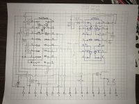
I drew the circuit around pin 10 and it seems to me that if pin 17 on the PS driver board is pulled low, pin 8 of the LM324 will be latched on, shutting the 594 down.
Should I try running it with Q1 removed so that this circuit is disabled and see what I get on pin 17?
I drew the circuit around pin 10 and it seems to me that if pin 17 on the PS driver board is pulled low, pin 8 of the LM324 will be latched on, shutting the 594 down.
Should I try running it with Q1 removed so that this circuit is disabled and see what I get on pin 17?
Attachments
Try lifting D5. Q1 could be leaky and this should show it.
You could also measure the voltage on the diode and transistor to see how they're being driven.
Where's the latching for the 324?
You could also measure the voltage on the diode and transistor to see how they're being driven.
Where's the latching for the 324?
The latching for the 324 is output (P8) goes high and charges C5 Through R9 and when it is higher than inverting input (P9) through R10 it latches on.
So there is a bit of a delay because of C5. (I guess if C5 is leaking badly that could also cause this symptom, but I would think that is unlikely).
I did pull Q1 and it seems fine, but I like the suggestion of pulling D5 and testing it that way in the circuit, brilliant!
I will report back! Thanks!
With D5 out of the circuit, the power supply is working as expected. Pin17 on the PS board is pulled low, so I have to investigate where that goes.
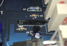
And it goes to mystery device number ANW12, a resistor network?
And it goes to mystery device number ANW12, a resistor network?
It is a network but they are typically custom made and can contain diodes.I don't have anything on that module but there are examples in the autotek folder of the tutorial.
Thanks Perry, I will trace that circuit and test any active components that may form part of the circuit first.
If you think the network is bad you can contact Zed Audio and he may have some since I bought one from him awhile back for an amp I was repairing .
Thank you caraudioguy! I have not had an opportunity to look at the amp again, but will report back, once I know more!
Thanks and Final Notes
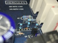
I wanted to give a shout out to Mr Stephen Mantz from Zed Audio that helped me by providing information and guidance. Below is a description that he provided of the ANW12, which he has replacements for in stock, if you need any.
The description of the ANW12 is:
Looking at the network with the 2 key pins on your right and now reading from left to right which I shall call pins 1-6 then a space and then pins 7 & 8.
I interpreted this description into the attached Diagram.
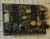
I implemented this with discrete components using 1/4W 1% Metal film resistors shown in the attached picture.
Thanks again for all the help from everyone!!
I wanted to give a shout out to Mr Stephen Mantz from Zed Audio that helped me by providing information and guidance. Below is a description that he provided of the ANW12, which he has replacements for in stock, if you need any.
The description of the ANW12 is:
Looking at the network with the 2 key pins on your right and now reading from left to right which I shall call pins 1-6 then a space and then pins 7 & 8.
- Pin 1-2 is a 4K3
- Pin 3 has a 100R to a 33K which is on pin 8 (so pin 8 through this 33K connects to pin 3). Pin 3 in addition has a 100R to pin 5
- Pin 4 has a 1N4148 diode to pin 5 with cathode at pin 4
- Pin 6 has a 10K to pin 7
I interpreted this description into the attached Diagram.
I implemented this with discrete components using 1/4W 1% Metal film resistors shown in the attached picture.
Thanks again for all the help from everyone!!
Attachments
- Home
- General Interest
- Car Audio
- HiFonics Hercules VIII have me beaten