Some history
At the latest 60s in Bulgaria there was an amplifier called “Studio 2 3x35Watts Hi-Fi Amplifier”. The manufacturer was a public manufacturer, and at that time (under the communism) there were limited components available to be used. One was the legendary 2N3055 Romanian or Bulgarian made. The rest of the components were BD139/140, 2T3552/3682, one KD504 and two BC337, and of course a minimalistic but lovely bootstrapped VAS. Very, very old school, so retro, so old fashion - you name it. And before couple of mounts I've heard that thing and I have lost my mind with it. This amplifier was indescribable - precise highs, flat and clear mids and deep powerful bass. I was not even thinking about to use the EQ … And on top of that the nominal supply voltage was just +/-32V, but I swear it sounds above that. That was my true expiration…
So here's the deal.
Some theoretical principals
A real audiophile's high fidelity amplifier has to meet some critical requirements, which are in relation with the human's common psycho-acoustical model. There are so many theories about them that everyone can get lost.
For example some of the engineers claim that the symmetry is essential, from the impute transistor couple, trough the VAS to the output.
There is also an opposite opinion, that claim the non symmetry is closer to the reality and gives more freedom to the designer, which I found is true.
That's why I am going to observe the practice [mine and other's], and to simply take those which are more involved in the ever lasting question - why the amplifiers are having similar parametric but in the same time are so differently sounding.
They are the well known issues: THD,TIMD, Power bandwidth, Dumping factor, Temperature and frequency/phase stability, simplicity, low cost, and so so ...
Most of the theorists claim that they are in a strong relation to each other. For example if you have low THD. So most commonly you have all other parametric within acceptable value. Well, that's the tricky moment. They are missing some extremely important parametric, and here they are: TIMD, phase shifting, dumping factor, fast response and the harmonic's structure. Also they're very difficult to be measured, due to its complexity. So the best way is to evaluate them while doing the scratch, with the irreplaceable assistance of the SPICE modeling.
Achieving low TIM distortions is not that easily as the low harmonic distortions. As a matter of fact in the practice they're in an opposite relation to each other. It's all about the proportion. The point were they equals is the "holly grail" for the audiophile's amplifier. However, lower TIMD means lower [but as flat as possible] open loop gain, and especially low [but high enough] margin between the open loop and the closed loop gain.
True distortion cancellation schematic is possible only if you're following two paths - feed-forward error correction or current negative feedback. The first one is more complicated and very often quite unstable with complexity of various frequency compensations. The second one is more attractive, because of its nature to be stable, giving in the same time very high slew rate, and is achieving amazingly low TIM distortion.
Of course there is a catch and when you use a true current feedback, the dumping is good, but limited to a lower point, in comparison with the voltage feedback topology, which of course leads to low efficiency.
So here comes the conclusion that if you use a global voltage feedback and local current feedback, you takes there advantages and you're avoiding there disadvantages. But how exactly this can happen? Here's how.
The input stage
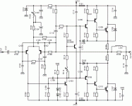
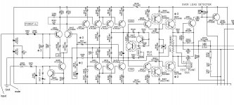
I preferred to use the long-tied input PNP-type transistor couple T101 and T102, loaded by a constant voltage generator, made by the zener diode D101 and some RC filters. There is also an option for additional adjustment (by turning R102), because of the manufacturing tolerance of the transistors. Instead of long tailed pair of transistor couple, for the upper and the lower side of the input stage. The advantages of that old school schematic are extremely important - essential frequency stability [oscillations free due to the limited gain], and a good harmonic's spread spectrum.
The VAS is extremely simple but by using a quality NPN transistor Q103 with good supply voltage margin [at least two times] the distortions are at it's minimum. The usage of Bootstrapped constant current load is for purpose - the limited bypass of the electrolytic capacitor is around 50 kHz which is very useful and it is kind of positive feedback giving additional linearization.
There's also additional 3-level frequency compensation. First the input, then the lag- and load- compensation, and third - the compensation in the NFB's loop, eliminating any possible instability issues. In addition there's a temperature compensating diodes for the VAS. No phase compensation is aloud, because of the dramatic decrease of the open loop bandwidth, just the input filter is responsible for the limited bandwidth.
The next stage is of course the final stage. It's the well known "Quad 303's triples". It's a "state of art" - a quasi complimentary topology giving unbeatable performance. The reason that I chose the quasi complimentary is that the market is overfilled with lots of fakes of very popular complimentary transistors, but on the other hand it is very easy to find a good and original TO-3s. For example ST, ON and Fairchild are still manufacturing them, and the storages have almost unlimited stock of TO-3s.
This final stage is even "amplifying" by voltage [thanks to the Ziklai-alike configuration] and the voltage drop is almost two times less. This is dramatically improving the dumping factor and the efficiency, additionally managing essential load control. Additional benefit is the "lack" of commutating distortions even in pure class B condition. To gain excellent distortion figure you need for the final transistors to conduct only 5-6 mA.
The protection plays two roles: by sensing the voltage drops over the power resistors and passing it trough the diodes [when the voltage exceeds the threshold forward voltage of the diodes] into the input of the triples. Simultaneously this "threshold" point changes with the temperature drift of the output transistors, giving good temperature compensation.
So the protection is simple, but very effective and the fuses are just in any case. The output current limit is set to around 4 amperes, which is quite enough for 4-ohms load.
I am not giving the values now, simply to make you honestly say what do you thing about that very unusual schematic. I’ll give them later. I thing that this can be the next most popular DIY project … unless I am totally wrong…
At the latest 60s in Bulgaria there was an amplifier called “Studio 2 3x35Watts Hi-Fi Amplifier”. The manufacturer was a public manufacturer, and at that time (under the communism) there were limited components available to be used. One was the legendary 2N3055 Romanian or Bulgarian made. The rest of the components were BD139/140, 2T3552/3682, one KD504 and two BC337, and of course a minimalistic but lovely bootstrapped VAS. Very, very old school, so retro, so old fashion - you name it. And before couple of mounts I've heard that thing and I have lost my mind with it. This amplifier was indescribable - precise highs, flat and clear mids and deep powerful bass. I was not even thinking about to use the EQ … And on top of that the nominal supply voltage was just +/-32V, but I swear it sounds above that. That was my true expiration…
So here's the deal.
Some theoretical principals
A real audiophile's high fidelity amplifier has to meet some critical requirements, which are in relation with the human's common psycho-acoustical model. There are so many theories about them that everyone can get lost.
For example some of the engineers claim that the symmetry is essential, from the impute transistor couple, trough the VAS to the output.
There is also an opposite opinion, that claim the non symmetry is closer to the reality and gives more freedom to the designer, which I found is true.
That's why I am going to observe the practice [mine and other's], and to simply take those which are more involved in the ever lasting question - why the amplifiers are having similar parametric but in the same time are so differently sounding.
They are the well known issues: THD,TIMD, Power bandwidth, Dumping factor, Temperature and frequency/phase stability, simplicity, low cost, and so so ...
Most of the theorists claim that they are in a strong relation to each other. For example if you have low THD. So most commonly you have all other parametric within acceptable value. Well, that's the tricky moment. They are missing some extremely important parametric, and here they are: TIMD, phase shifting, dumping factor, fast response and the harmonic's structure. Also they're very difficult to be measured, due to its complexity. So the best way is to evaluate them while doing the scratch, with the irreplaceable assistance of the SPICE modeling.
Achieving low TIM distortions is not that easily as the low harmonic distortions. As a matter of fact in the practice they're in an opposite relation to each other. It's all about the proportion. The point were they equals is the "holly grail" for the audiophile's amplifier. However, lower TIMD means lower [but as flat as possible] open loop gain, and especially low [but high enough] margin between the open loop and the closed loop gain.
True distortion cancellation schematic is possible only if you're following two paths - feed-forward error correction or current negative feedback. The first one is more complicated and very often quite unstable with complexity of various frequency compensations. The second one is more attractive, because of its nature to be stable, giving in the same time very high slew rate, and is achieving amazingly low TIM distortion.
Of course there is a catch and when you use a true current feedback, the dumping is good, but limited to a lower point, in comparison with the voltage feedback topology, which of course leads to low efficiency.
So here comes the conclusion that if you use a global voltage feedback and local current feedback, you takes there advantages and you're avoiding there disadvantages. But how exactly this can happen? Here's how.
The input stage
I preferred to use the long-tied input PNP-type transistor couple T101 and T102, loaded by a constant voltage generator, made by the zener diode D101 and some RC filters. There is also an option for additional adjustment (by turning R102), because of the manufacturing tolerance of the transistors. Instead of long tailed pair of transistor couple, for the upper and the lower side of the input stage. The advantages of that old school schematic are extremely important - essential frequency stability [oscillations free due to the limited gain], and a good harmonic's spread spectrum.
The VAS is extremely simple but by using a quality NPN transistor Q103 with good supply voltage margin [at least two times] the distortions are at it's minimum. The usage of Bootstrapped constant current load is for purpose - the limited bypass of the electrolytic capacitor is around 50 kHz which is very useful and it is kind of positive feedback giving additional linearization.
There's also additional 3-level frequency compensation. First the input, then the lag- and load- compensation, and third - the compensation in the NFB's loop, eliminating any possible instability issues. In addition there's a temperature compensating diodes for the VAS. No phase compensation is aloud, because of the dramatic decrease of the open loop bandwidth, just the input filter is responsible for the limited bandwidth.
The next stage is of course the final stage. It's the well known "Quad 303's triples". It's a "state of art" - a quasi complimentary topology giving unbeatable performance. The reason that I chose the quasi complimentary is that the market is overfilled with lots of fakes of very popular complimentary transistors, but on the other hand it is very easy to find a good and original TO-3s. For example ST, ON and Fairchild are still manufacturing them, and the storages have almost unlimited stock of TO-3s.
This final stage is even "amplifying" by voltage [thanks to the Ziklai-alike configuration] and the voltage drop is almost two times less. This is dramatically improving the dumping factor and the efficiency, additionally managing essential load control. Additional benefit is the "lack" of commutating distortions even in pure class B condition. To gain excellent distortion figure you need for the final transistors to conduct only 5-6 mA.
The protection plays two roles: by sensing the voltage drops over the power resistors and passing it trough the diodes [when the voltage exceeds the threshold forward voltage of the diodes] into the input of the triples. Simultaneously this "threshold" point changes with the temperature drift of the output transistors, giving good temperature compensation.
So the protection is simple, but very effective and the fuses are just in any case. The output current limit is set to around 4 amperes, which is quite enough for 4-ohms load.
I am not giving the values now, simply to make you honestly say what do you thing about that very unusual schematic. I’ll give them later. I thing that this can be the next most popular DIY project … unless I am totally wrong…
Attachments
Kostazl,
Lot thanks for posting this schematic and thanks for your comment on it. This's a lovely design for me!
I'm from Hungary, not very far from Bulgaria. We were under the pressure of the Soviet regime too, so here we used old-fashioned schematics too with cheap and simple parts as your schematic does.
And I prefer these designs in this modern days too! Now there is democracy in Bulgaria and Hungary, with modern semiconductors etc... 🙂 But the amplifiers from the previous regime are excellent, nowadays too! Many times I feel these old-fashined amplifiers using 2N3055, bootstrapped VAS, etc... are sounding better than the modern 0.00001%-THD so called "audiophile" amplifiers.
So please keep on work, I love these amplifiers!
And please post us the parts list if you can.
Regards,
Dzsoni
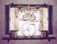
Photo of a 2×250W PA-amplifier using Checzslovakian Tesla-KD502 as output transistors in serial-quasicomplementray arrangement, driven by some BD137. Made in Hungary in the 80's.
Sorry it's not HiFi but a nice "socialist" type PA-amplifier. These amplifiers are working nowadays too, without any faults or problems!
Really workhorses with cheap parts.
Regards,
PS.: This "Studio 35W" amplifier would be a nice DIY-project!
Sorry it's not HiFi but a nice "socialist" type PA-amplifier. These amplifiers are working nowadays too, without any faults or problems!
Really workhorses with cheap parts.
Regards,
PS.: This "Studio 35W" amplifier would be a nice DIY-project!
Attachments
Hi kostazl,
What are the purposes of R105 and R115? Shouldn't C105 have a series resistor?
I do have to disagree with you about this being an unusual schematic. 😀
What are the purposes of R105 and R115? Shouldn't C105 have a series resistor?
I do have to disagree with you about this being an unusual schematic. 😀
My guess is D104 and D105 prevent excessive reverse biasing and possible breakdown of Q105 and Q108 ?
The schematic provided may sound great
Someone will have to be very bad to destroy this topologie sonics.
I cannot believe this one will sound sound bad.
Very nice schematics.... socialist block had very good amplifiers we could see researching the internet.
Very good that we have all of you around us now a days.... more pictures please...show us what old socialist block was doing those last fourty years.
regards,
Carlos
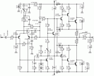
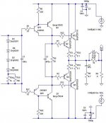
Well, firstly this is not the original schematic, but it’s based on it. D102 and D103 is a thermal compensation for the VAS, and they are necessary, because the Bootstrap loader cannot compensate the thermal drift of Q103 /with other words the diodes are in any case/. R105 is limiting the gain of the input stage and R115 is limiting the VAS gain, so the global open loop gain is flat until 20 kHz. Soon I will post the original schematic of the amplifier…
Here is a part of the original schematic (the final stage). I am also ready with the PCB. By the way, D104 and D105 are acting as an over current protection, as well as a thermal compensation, so there is no any temperature sensing component on the heat sink. Believe it or not, the original amplifier is unbelievably cool…
Attachments
The input (most right part of schematic), is referenced to negative rail? Shouldn't the lower leg of R1601 (VR25K) is connected to ground?
The idea for R1601 is to adjust the input bias point by changing the resistance of the grounding input resistor (to change the input resistance and the input offset). This is what I don’t like in the original schematic, because sometimes this adjustment is doing nothing, so I added a better way to precisely set the input offset and eliminate the influence of the difference in the hfe of Q101 and Q102
Well, the original amp sounds excellent, very neutral (no stupid “colorization”), linear, with very clean and detail trebles and mids and it’s very, very loud at the same time. But there was a noise and a high nonadjustable offset at the output (around 150 mV), and I thing slight oscillations. So I fixed the problems by redesigning the input, the VAS and the Triples. To be honest, the input stage and the VAS are very similar to the “Natural sound amplifier” topology of Yamaha. And the triples are from the well known Quad303. I did not see any combination like this, so Studio 2 inspired me to do it. That makes it A VERY UNIQUE AMPLIFIER, by the way.
I used Multisim 9 and my modification was much better than Studio 2. I have tried so many variations, and every time I was finishing at the point were I started…
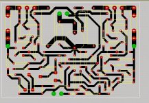
So I will give you the prototype of the PCB. The output transistors are wired to the heatsink. I want somebody to build it with me, to find the optimum. Wanna to try?...
I used Multisim 9 and my modification was much better than Studio 2. I have tried so many variations, and every time I was finishing at the point were I started…
So I will give you the prototype of the PCB. The output transistors are wired to the heatsink. I want somebody to build it with me, to find the optimum. Wanna to try?...
Attachments
kostazl said:Here are the parts and their nominal values. There was a small mistake at the first schematic, so now it is fixed. The nominal power supply is between +/-30 and 35V.
I think it would sound like exploding electrolytic capacitors, wouldn't it?
+ -|(-
..Todd
Hi, dear Kostazl, good night.Some history
At the latest 60s in Bulgaria there was an amplifier called “Studio 2 3x35Watts Hi-Fi Amplifier”. The manufacturer was a public manufacturer, and at that time (under the communism) there were limited components available to be used. One was the legendary 2N3055 Romanian or Bulgarian made. The rest of the components were BD139/140, 2T3552/3682, one KD504 and two BC337, and of course a minimalistic but lovely bootstrapped VAS. Very, very old school, so retro, so old fashion - you name it. And before couple of mounts I've heard that thing and I have lost my mind with it. This amplifier was indescribable - precise highs, flat and clear mids and deep powerful bass. I was not even thinking about to use the EQ … And on top of that the nominal supply voltage was just +/-32V, but I swear it sounds above that. That was my true expiration…
So here's the deal.
Some theoretical principals
A real audiophile's high fidelity amplifier has to meet some critical requirements, which are in relation with the human's common psycho-acoustical model. There are so many theories about them that everyone can get lost.
For example some of the engineers claim that the symmetry is essential, from the impute transistor couple, trough the VAS to the output.
There is also an opposite opinion, that claim the non symmetry is closer to the reality and gives more freedom to the designer, which I found is true.
That's why I am going to observe the practice [mine and other's], and to simply take those which are more involved in the ever lasting question - why the amplifiers are having similar parametric but in the same time are so differently sounding.
They are the well known issues: THD,TIMD, Power bandwidth, Dumping factor, Temperature and frequency/phase stability, simplicity, low cost, and so so ...
Most of the theorists claim that they are in a strong relation to each other. For example if you have low THD. So most commonly you have all other parametric within acceptable value. Well, that's the tricky moment. They are missing some extremely important parametric, and here they are: TIMD, phase shifting, dumping factor, fast response and the harmonic's structure. Also they're very difficult to be measured, due to its complexity. So the best way is to evaluate them while doing the scratch, with the irreplaceable assistance of the SPICE modeling.
Achieving low TIM distortions is not that easily as the low harmonic distortions. As a matter of fact in the practice they're in an opposite relation to each other. It's all about the proportion. The point were they equals is the "holly grail" for the audiophile's amplifier. However, lower TIMD means lower [but as flat as possible] open loop gain, and especially low [but high enough] margin between the open loop and the closed loop gain.
True distortion cancellation schematic is possible only if you're following two paths - feed-forward error correction or current negative feedback. The first one is more complicated and very often quite unstable with complexity of various frequency compensations. The second one is more attractive, because of its nature to be stable, giving in the same time very high slew rate, and is achieving amazingly low TIM distortion.
Of course there is a catch and when you use a true current feedback, the dumping is good, but limited to a lower point, in comparison with the voltage feedback topology, which of course leads to low efficiency.
So here comes the conclusion that if you use a global voltage feedback and local current feedback, you takes there advantages and you're avoiding there disadvantages. But how exactly this can happen? Here's how.
The input stage
I preferred to use the long-tied input PNP-type transistor couple T101 and T102, loaded by a constant voltage generator, made by the zener diode D101 and some RC filters. There is also an option for additional adjustment (by turning R102), because of the manufacturing tolerance of the transistors. Instead of long tailed pair of transistor couple, for the upper and the lower side of the input stage. The advantages of that old school schematic are extremely important - essential frequency stability [oscillations free due to the limited gain], and a good harmonic's spread spectrum.
The VAS is extremely simple but by using a quality NPN transistor Q103 with good supply voltage margin [at least two times] the distortions are at it's minimum. The usage of Bootstrapped constant current load is for purpose - the limited bypass of the electrolytic capacitor is around 50 kHz which is very useful and it is kind of positive feedback giving additional linearization.
There's also additional 3-level frequency compensation. First the input, then the lag- and load- compensation, and third - the compensation in the NFB's loop, eliminating any possible instability issues. In addition there's a temperature compensating diodes for the VAS. No phase compensation is aloud, because of the dramatic decrease of the open loop bandwidth, just the input filter is responsible for the limited bandwidth.
The next stage is of course the final stage. It's the well known "Quad 303's triples". It's a "state of art" - a quasi complimentary topology giving unbeatable performance. The reason that I chose the quasi complimentary is that the market is overfilled with lots of fakes of very popular complimentary transistors, but on the other hand it is very easy to find a good and original TO-3s. For example ST, ON and Fairchild are still manufacturing them, and the storages have almost unlimited stock of TO-3s.
This final stage is even "amplifying" by voltage [thanks to the Ziklai-alike configuration] and the voltage drop is almost two times less. This is dramatically improving the dumping factor and the efficiency, additionally managing essential load control. Additional benefit is the "lack" of commutating distortions even in pure class B condition. To gain excellent distortion figure you need for the final transistors to conduct only 5-6 mA.
The protection plays two roles: by sensing the voltage drops over the power resistors and passing it trough the diodes [when the voltage exceeds the threshold forward voltage of the diodes] into the input of the triples. Simultaneously this "threshold" point changes with the temperature drift of the output transistors, giving good temperature compensation.
So the protection is simple, but very effective and the fuses are just in any case. The output current limit is set to around 4 amperes, which is quite enough for 4-ohms load.
I am not giving the values now, simply to make you honestly say what do you thing about that very unusual schematic. I’ll give them later. I thing that this can be the next most popular DIY project … unless I am totally wrong…
I speeking from Brasil, and i see you post from 2007, about the Bulgarian “Studio 2 3x35Watts Hi-Fi Amplifier”. And i really crazy about it.
Hi-Fi Class B Amplifier
And want to know, if you could help me, of course.
Is this an easy amplifier to built?
I have no experience building amplifiers, but i very samrt for this kind of stuff. And i can solder pretty well. And if with those GIF image you atteched on topic, called "303", i can know everything i need to built one of this. I have a hybrid amplifier (tube pre and mosfet on amplifier, from a brazilian legendary company, called Audiopax), and i like it very much, and the detail is that this amplifier i have is class B too, and have an amazing sound, really amazing. This instigate me to search for another class B, and than i find you.
Anyway, i want to know this, and if you have made one of this for you, and if you have any photos to show me.
My e-mail is Email address deleted by moderation as requested.
Best regards, cheers from Brasil
- Status
- Not open for further replies.
- Home
- Amplifiers
- Solid State
- Hi-Fi Class B Amplifier