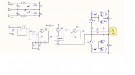
MOSFET driver is Q4,5,6,7.
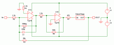
U1A: integrator, U1B: histeretic comparator. Basically it works like an NE555. C9 is charged until the comparator reaches the threshold, it changes the output polarity, and the capacitor starts to discharge (because of the current from R16). Input voltage makes discharging faster and charging slower (for positive input ploarity), so modifies duty cycle.
Feedback and integrator works as the usual 1st order feedback loop also, keep distortion low.
I quess you mean "two different".
Different MOSFETs are used because positive rail is different polarity from negative rail. N-channel MOSFET for negative, p-channel for positive. N-channel for positive is more complicated.
U1A: integrator, U1B: histeretic comparator. Basically it works like an NE555. C9 is charged until the comparator reaches the threshold, it changes the output polarity, and the capacitor starts to discharge (because of the current from R16). Input voltage makes discharging faster and charging slower (for positive input ploarity), so modifies duty cycle.
Feedback and integrator works as the usual 1st order feedback loop also, keep distortion low.
why it use to different mosfets
I quess you mean "two different".
Different MOSFETs are used because positive rail is different polarity from negative rail. N-channel MOSFET for negative, p-channel for positive. N-channel for positive is more complicated.
When the output of U1B goes positive, Q1 switches on, pulling it's collector voltage down. This switches Q5 and M1 on, pulling the output voltage up.
At the same time, Q2 is switched off and current through R6 switches Q4 on. Q4 pulls the voltage on the gate of M2 down to switch it off fast.
Similarly, when the output of U1B goes negative M2 is switched on, M1 is switched off, and the output voltage goes down.
At the same time, Q2 is switched off and current through R6 switches Q4 on. Q4 pulls the voltage on the gate of M2 down to switch it off fast.
Similarly, when the output of U1B goes negative M2 is switched on, M1 is switched off, and the output voltage goes down.
hi guys is the function of UD is a differentiation op amp or what cause i do not understand how TL074 behave
Yes they do! I only explained one half of the operation in detail, and hoped you would understand that the other half is similar. Here is the other half of the explanation in detail:oh ok .. so Q3 and Q6 do not have function
When the output of U1B goes negative, Q2 switches on, pulling it's collector voltage up. This switches Q6 and M2 on, pulling the output voltage down.
At the same time, Q1 is switched off and current through R5 switches Q3 on. Q3 pulls the voltage on the gate of M1 up to switch it off fast.
TL074 is a quad opamp. That means it is one integrated circuit containing four opamps. In your circuit, U1A is an opamp, U1B is an opamp, U1C is an opamp, and U1D is an opamp. Each one is just a normal opamp, but they are used in different ways.i do not understand how TL074 behave
~~~~~~~~~~~~~~~~~~~~~~~~~~~~~~~~~~~~~~~~~~~~~~
Class D is the most difficult kind of amplifier to understand. You don't seem to know much about electronics. This is a bad combination.
Why do you want to make a class D amplifier in one week?
Wouldn't it be better to start with something easier?
YEAH I KNOW I HAVE LITTLE INFO ABOUT ELECTRONICS BUT I M INTEREST IN CLASS D ....what i mean when i said i do not understand TL074 behavior i mean in this circuit how it is operated
C1, C2, R18, R23 and R24 are all marked "DNP". Does that mean "Do Not Place", or something else?is the function of UD is a differentiation op amp or what
If those parts are left out then U1D is a unity gain buffer. If those parts are included then U1D has some gain and the frequency response will be changed.
Where on this forum did you find the circuit? Maybe there is other information there that can help. Can you give a link?
oh ... yeah i got it from this forums and this the link http://www.diyaudio.com/forums/class-d/205654-ultra-simple-class-d.html
Thanks. From the attachment:
Google translate =>Los componentes con valor DNP no deben colocarse (son para experimentos)
So U1D is just a buffer.DNP-value components should not be placed (they are for experiments)
oh thanks .... so that mean U1D is just buffer and U1A is integrator which will change the PWM feedback from the power stage to triangle wave apply to U1B which is a comparotor and the output of U1B is PWM .... is that ryt
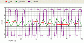
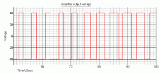
Yes. Here's some pictures to show the voltage at the outputs of U1A and U1B, with 20KHz input signal..... is that ryt
Attachments
😕 Where are they? I can only see D3, D4, D5 and D6. Sometimes numbers go missing when you add components to a schematic, then delete them.
- Status
- Not open for further replies.
- Home
- Amplifiers
- Class D
- hi can anyone help me with this circuit