@Mooly:
😛 ... Well now, I don't exactly know what a masthead amp is but I see before me something like the antennas transmitting mobile phone signals ... I am simply not sure I can make my DAC big enough to enable hand-held measurements with such an amplifier 😉
😀 Small TV aerial amplifiers that bolt directly to the mast. The input impedance would be a bit low. FET buffer in front maybe... just daft ideas 😛
@Mooly
@RJM:
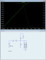
Hi, & thanks for your comment on this and the link ... I'm actually not quite clear on what happens here but when I simulate the circuitry with the capacitor placed the way I've done it in the schematic (you've reversed them in your schematic) the simulation comes out like shown in the attachment.
Reasoning about it, the capacitance of the 1n4148 is ~4pF so the series/parallel combination will give ~ 2.6 pF. 50 ohms in series with 2.6 pF gives a -3 dB point at ~1.2 GHz ... But to be honest I don't quite know what happens since the simulations are different ???
Greetings,
Jesper
... Yups, figured that out 😉just daft ideas
@RJM:
With the 1N4148’s at your input, the capacitance of the diodes will put you down about 9db at 100MHZ.
Hi, & thanks for your comment on this and the link ... I'm actually not quite clear on what happens here but when I simulate the circuitry with the capacitor placed the way I've done it in the schematic (you've reversed them in your schematic) the simulation comes out like shown in the attachment.
Reasoning about it, the capacitance of the 1n4148 is ~4pF so the series/parallel combination will give ~ 2.6 pF. 50 ohms in series with 2.6 pF gives a -3 dB point at ~1.2 GHz ... But to be honest I don't quite know what happens since the simulations are different ???
Greetings,
Jesper
Attachments
Last edited:

@RJM1:
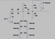
Hi & thanks for commenting. And yes, I can see what you mean ... Just checked the datasheet and the 1N4148 already conducts 0.01 mA around 0.4 volts forward voltage so unless I'd like to add some more 1N4148s I'll have to find another solution.
Might one of you have ideas here? Preferably very low capacity and no conduction at 5 volts forward voltage.
Thanks again RJM1 ;-)
Jesper
The problem is that D1,2,3 are conducting.
Hi & thanks for commenting. And yes, I can see what you mean ... Just checked the datasheet and the 1N4148 already conducts 0.01 mA around 0.4 volts forward voltage so unless I'd like to add some more 1N4148s I'll have to find another solution.
Might one of you have ideas here? Preferably very low capacity and no conduction at 5 volts forward voltage.
Thanks again RJM1 ;-)
Jesper
@DUG:
Well, yes, but the LMH6629 doesn't simulate as well (by a good margin) on split supplies, especially not at HF. Also, I'd have to make for two supplies, and still would have to include capacitors in the input and diodes both ways. I've considered this solution as well but didn't find it to work as well as the single supply version .... 😱
Jesper
Change to split supplies.
A lot of your DC issues will be negated.
Well, yes, but the LMH6629 doesn't simulate as well (by a good margin) on split supplies, especially not at HF. Also, I'd have to make for two supplies, and still would have to include capacitors in the input and diodes both ways. I've considered this solution as well but didn't find it to work as well as the single supply version .... 😱
Jesper
In your post # 22 switch the places of R1 and C1 and place your diodes after the resistor but before the capacitor.
@RJM1:
Hi - thanks for the idea but if I interprete your suggestion correctly it would mean that if there's a DC component on the input to the circuitry the DC voltage would drop down through the 50 ohm resistor and the diodes ... Which won't work as I'd like to be able to measure signals with a DC component.
Best regards,
Jesper
In your post # 22 switch the places of R1 and C1 and place your diodes after the resistor but before the capacitor.
Hi - thanks for the idea but if I interprete your suggestion correctly it would mean that if there's a DC component on the input to the circuitry the DC voltage would drop down through the 50 ohm resistor and the diodes ... Which won't work as I'd like to be able to measure signals with a DC component.
Best regards,
Jesper
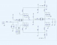
Hi all,
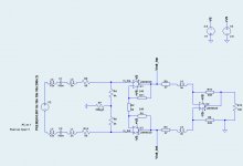
In hoping that this ends up being a good solution - with due thanks to your inputs 😉 - this is the schematic that I've now drawn up. Changes are single -> dual supplies, fewer diodes on the input and moving the placement of the diodes.
The circuitry simulates straight from ~8 kHz to appr. 140 MHz - but - with a 25 ohm resistor on the output to the cable leading to the oscilloscope. What really decides the bandwidth limit here is the resistor value on the output to the cable leading to the oscilloscope - I've calculated with 30 pF (RG-58 cable) capacitance from the cable, however, if one of you know of a lower capacitance cable that can be bought in practice (Mouser, Digikey) ... 🙂
Both the input capacitor, resistor & diodes may experience a quite high pulse current when connecting to the DUO's (Device Under Observation) rail voltage, however, so they should be able to handle such current (~600 mA at 30 VDC rail voltage, 10ns pulse rise time).
Also, I hope that the 50 ohms resistors to ground on both outputs are not needed as they reduce the effective amplification of the circuitry (40 dBs if not there). The amplification could be increased to compensate for this but doing so reduces the bandwidth.
So this is where it is - if you have suggestions for improvements please feel welcome to comment ...
Greetings,
Jesper
Attachments
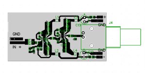
Hi again 😉,
I've now drawn up a PCB layout which I hope to progress with shortly. It's based on the schematic posted just above (and in this post as well) and has a top signal layer and a bottom GND layer. I've chosen to not fill the top layer with copper as TI does not do so in their EVM board.
Any comments on improving the layout is welcome especially about where to place the vias that connect the signal layer GND traces to the bottom layer GND plane. Ideally, as I understand this, to have low inductance signal & gnd should run just next to eachother, however, to me it looks as if this is not just easy to accomplish. Also, since I will be hand-soldering the board I cannot place vias below the LMH6629's as I reckon doing so could make soldering the LMH6629 onto the board "a challenge".
To the left of the PCB board there are two pads onto which I'll solder two isolated pins of ~12 mm length. Those will be the pins I use to measure the circuitry in question. To the right there's a BNC connector connecting the board to the oscilloscope. Also to the right are 4 pads used to connect 4 NiMH batteries to the board.
The top side of the board will be shielded with either a copper foil shield or some of the metal used to shield harddisks.
Although I was inspired by the a modified instrumentation amplifier approach to the circuitry (last attachment - courtesy Bruno Putzeys) I had already ordered the components so maybe some other time ...
Greetings,
Jesper
Attachments
Gain RF and proximity is a tough combination to deal with. Further wide bandwidth makes the intrinsic noise higher. You are looking for more than 40 dB of gain over a wide bandwidth. Usually you need really good shielding between stages to get that to work. There is reason that scopes with wide bandwidth rarely go to less than 10 mV/division. Some that do limit the bandwidth for the higher gains.
What I would do is use something from these guys: Mini-Circuits Amplifiers like this : http://www.minicircuits.com/pdfs/ZFL-1000LN+.pdf or this : http://www.minicircuits.com/pdfs/RAM-8A+.pdf but I'm really lazy.
At 100 MHz this stuff works way differently than audio.
First calculation- 100 Ohm source Z = 12 uV of thermal noise. If the source impedance is higher the noise will be higher. A Tex 7a13 goes down to 1 mV with 100 MHz bandwidth (the highest gain wideband solution I know of). Under those conditions (1 mV 150 MHz BW, input shorted) the noise is 1/2 division. I think you will find with more that 20 dB more gain all you will get is a screen full of noise.
The more constructive way to look at wideband noise (and find its sources) is a spectrum analyzer. I just discovered this: RF Explorer - 3G Combo [TES09102P] - $269.00 : Seeed Studio Bazaar, Boost ideas, extend the reach which I think would be a more useful tool. Much easier to deal with than my old Tek 7S12.
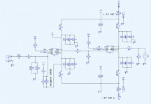
@gootee: Yes, of course. I've added the schematic with component designators to this post.
@1audio: Hi Demian ... thanks for your feedback - I find it very useful although I would have hoped "to get it earlier" - before ordering the components for the amplifier 😱. However, to follow up on your feedback I reply in the depth I can below.
However, apparently one of them is this:
To try to follow your line of thinking: The source impedance usually would be low (digital PSU measurements, I/V converter circuitry, PSUs in general, low impedance amplifier circuitries) and with about 40 dBs of gain the 12 uV (15 uVs with 150 MHz bandwidth) would become 1.2 mV. This will be referenced to the noise signal that I'm measuring which will then also be amplified a 100 times ... Wouldn't that work with a reasonable practical resolution? The noise is ~ random (as I understand it) so should have no "shape" as would often be the case with the noise signal I intend to measure.
However, your comment makes me realize that maybe I should have used an AD8099 instead ... The LMH6629 needs a minimum of 25 ohms on the non-inverting input (I will change the 50 ohms to 25 ohms) which the AD8099 as far as I can see doesn't. This could lower input noise in practice. On the other hand the LMH6629 has a very clean square wave reproduction which is why I chose it over the AD8099. So many options ...
Thanks again for commenting, Demian ... I'd also appreciate your further comments on my questions/remarks if possible. Not least if you reckon it wouldn't work.
Greetings,
Jesper
@1audio: Hi Demian ... thanks for your feedback - I find it very useful although I would have hoped "to get it earlier" - before ordering the components for the amplifier 😱. However, to follow up on your feedback I reply in the depth I can below.
This is actually what I'm hoping to do using my Rigol oscilloscope's somewhat crude spectrum analyzer. However, its resolution is 2 mV/div and I'd appreciate going lower than that, if possible. Hence this HF amplifier (which of course needs to work as intended).The more constructive way to look at wideband noise (and find its sources) is a spectrum analyzer.
Yup, I'm in the process of realizing this although I don't yet know what the nuanced implications are .... (While at it do you know of a source for HF/RF amplifier design which is easy to understand and not overly formula oriented? E.g. written in a style similar to Howard Johnson's "High Speed digital design" .. )At 100 MHz this stuff works way differently than audio.
However, apparently one of them is this:
Do you think it would help to shield the two stages separately with the crossover point being R6 + R7? I have some copper sheet (0.2 mm) that I can cut for this and e.g. solder to a rim of a gnd trace that I can add to the top layer of the PCB.Usually you need really good shielding between stages to get that to work.
Hmmm... if realistic I'd prefer to progress with this design but just in case I need an alternative this looks very interesting (although I assume it has a 50 ohms input resistance/impedance?). Might you know where to buy it in low Nos and without substantial fees (20 seems to be the minimum from mini circuits)?http://www.minicircuits.com/pdfs/RAM-8A+.pdf but I'm really lazy.
Well, that indeed wouldn't be my objective 😛First calculation- 100 Ohm source Z = 12 uV of thermal noise. If the source impedance is higher the noise will be higher. A Tex 7a13 goes down to 1 mV with 100 MHz bandwidth (the highest gain wideband solution I know of). Under those conditions (1 mV 150 MHz BW, input shorted) the noise is 1/2 division. I think you will find with more that 20 dB more gain all you will get is a screen full of noise.
To try to follow your line of thinking: The source impedance usually would be low (digital PSU measurements, I/V converter circuitry, PSUs in general, low impedance amplifier circuitries) and with about 40 dBs of gain the 12 uV (15 uVs with 150 MHz bandwidth) would become 1.2 mV. This will be referenced to the noise signal that I'm measuring which will then also be amplified a 100 times ... Wouldn't that work with a reasonable practical resolution? The noise is ~ random (as I understand it) so should have no "shape" as would often be the case with the noise signal I intend to measure.
However, your comment makes me realize that maybe I should have used an AD8099 instead ... The LMH6629 needs a minimum of 25 ohms on the non-inverting input (I will change the 50 ohms to 25 ohms) which the AD8099 as far as I can see doesn't. This could lower input noise in practice. On the other hand the LMH6629 has a very clean square wave reproduction which is why I chose it over the AD8099. So many options ...
Thanks again for commenting, Demian ... I'd also appreciate your further comments on my questions/remarks if possible. Not least if you reckon it wouldn't work.
Greetings,
Jesper
Attachments


Hello, my first comment would be to via everything down to the ground and avoid ground connections on the top layer.
I will look in more detail in a bit, but I am almost back in the land of the sane and healthy...
See ya soon.
I will look in more detail in a bit, but I am almost back in the land of the sane and healthy...
See ya soon.
I would never have dreamed of progressing a project like this without first bread-boarding it on to blank copper board, "dead-bug" style.
@marce: Thanks for the suggestion - I'll look into it Monday. Get well(er) soon ;-)
@cliffforest: Hi ... I have a PCB making setup so it's actually easier for me to do it this way. Also I reckon by having a pcb as such shielding & shorter tracks are easier to accomplish. But thanks for considering ...
Greetings,
Jesper
@cliffforest: Hi ... I have a PCB making setup so it's actually easier for me to do it this way. Also I reckon by having a pcb as such shielding & shorter tracks are easier to accomplish. But thanks for considering ...
Greetings,
Jesper
Typically you don't use feedback amps like the CFB or VFB opamps for this type of application. However keeping the stage gain modest (10X max) seems to work. Adding an adjustable attenuator between the two stages may make it more usable (most Tek preamps have that type of construction to maintain dynamic range).
I would provide for a shield between the stages. A simple copper plate may be enough.
The Minicircuits stuff is interesting because you can buy just one. At 100 MHz your input Z is low anyway. Use a probe to manage the interface. Probing high frequencies is not a simple thing either. You need to keep the tip and return in close proximity to get a decent measurement. There is a lot on this you can look at on the web. You may want to build an active probe to see what you are looking for. This looks good: http://elektrotanya.com/files/forum/2009/10/e04a036.pdf
Have you experimented with the fft on the scope? You may find it can see well below the 5 mV / div that the waveform display is showing. Even the 8 bit ADC's are good enough to see 40-60 dB down. And think through what you will do with what you find. Some things like clock feedthrough to the power supply will never be completely removed.
- Status
- Not open for further replies.
- Home
- Design & Build
- Equipment & Tools
- HF add-on amplifier to my oscilloscope + probes