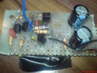
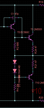
Hi, i built this and the 22 ohm resistors start to burn, protecting the bc560 from death 
 .
.
Any suggestions why not working, frying T5 ?
Im using 2n7000 mosfets instead bc547.
.Any suggestions why not working, frying T5 ?
Im using 2n7000 mosfets instead bc547.
Attachments
Last edited:
Using mosfets instead of the required bipolar devices is like fitting a Mini Cooper wheels on a Ford Mustang.
You can't go because the Mustang is sitting on its oil sump.
Suggest you use the correct bipolar devices . . .
You can't go because the Mustang is sitting on its oil sump.
Suggest you use the correct bipolar devices . . .
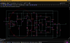
OK, there are many sub-optimal things in the circuit, but the main question again - how do you choose the quiescent currents for the cascades?
T5 quiescent current is around 1mA (a bit low to my taste), the one through T3, T10 - around 10mA (this is rather a lot for TO-92 transistors). You don't see it in the simulator, but in real life these two will be rather hot.
Although, having all this, 22R should not be burning, so there is something wrong in your implementation. Are you sure all the transistors are soldered the right way? BC5XX and 2N5XXX have got different pinouts (just in case)...
yes im sure .. 🙁 with 1ma gived best distortion result.
how they getting hot ? i am pushing them to 1/2 of their Pd limit 625mw ?
how they getting hot ? i am pushing them to 1/2 of their Pd limit 625mw ?
Last edited:
how they getting hot ? i am pushing them to 1/2 of their Pd limit 625mw ?
High frequency oscillation?
Use a solderless breadboard to develop the circuit. It's a lot easier to work on that way.
https://learn.sparkfun.com/tutorials/how-to-use-a-breadboard
Last edited:
47p is not enough for compensation ?
and vzaichenko meant they will get hot under normal operation.
my breadboard is busy now and cant use it. also i dont have other transistors to play with.
also breadboard is full of capacitaneces and dont want to use it with such a sensitive task.
when i mentioned "im sure" i meant im sure for the pinouts, i know they are different. not about current that im sure 1ma is the best.
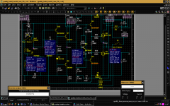
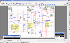
i added attach where i drawed the components in paint, open in full size to see the drawings.
and vzaichenko meant they will get hot under normal operation.
my breadboard is busy now and cant use it. also i dont have other transistors to play with.
also breadboard is full of capacitaneces and dont want to use it with such a sensitive task.
yes im sure .. 🙁
when i mentioned "im sure" i meant im sure for the pinouts, i know they are different. not about current that im sure 1ma is the best.
i added attach where i drawed the components in paint, open in full size to see the drawings.
Attachments
Last edited:
R4 sets that current at about 9-10 mA. Yes?
R2 sets Vbe of T3 at about 6.8V...if it could get there.
So actually most of the 9-10mA is going to be base current for T3
What is current gain of T3?
That is the current through 22R...more or less.
Close?
Added note: IMHO running something at 50% of rating better have some kind of heat sink.
R2 sets Vbe of T3 at about 6.8V...if it could get there.
So actually most of the 9-10mA is going to be base current for T3
What is current gain of T3?
That is the current through 22R...more or less.
Close?
Added note: IMHO running something at 50% of rating better have some kind of heat sink.
The 22r resistors are undespecified, that's it.Hi, i built this and the 22 ohm resistors start to burn, protecting the bc560 from death .hepl me please, need fast help
Suggest you use
RH05022R00FE02 Vishay / Dale | Mouser
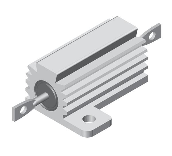
If not enough, this 1800kW (not a typo) water cooled one:

can take anything you can throw at it.
This is probably good enough.
Online Shop 3W Watt 22 ohm 22ohm 22R Metal Film Resistor 3 W +/-1% 10pcs|Aliexpress Mobile
That 1800kw looks kind of like a process air heater I used to use. It could heat air flows of 0.1lbm/Sec up to 1100F. I think it was way more watts though - looked just like that though.
Online Shop 3W Watt 22 ohm 22ohm 22R Metal Film Resistor 3 W +/-1% 10pcs|Aliexpress Mobile
That 1800kw looks kind of like a process air heater I used to use. It could heat air flows of 0.1lbm/Sec up to 1100F. I think it was way more watts though - looked just like that though.
The 22r resistors are undespecified, that's it.
Suggest you use
RH05022R00FE02 Vishay / Dale | Mouser
If not enough, this 1800kW (not a typo) water cooled one:
An externally hosted image should be here but it was not working when we last tested it.
can take anything you can throw at it.
😀
Guys, what are you talking about?
In normal operation, the current through those 22R resistors is roughly 12mA.
Simple calculation (P=I*I*R) gives us dissipation of 3.1mW on those resistors.
Even 1/8W will work fine there.
The point - it's far from normal operation...
OK - you asked for it.
Look at the way your dynamic load is organized (T10).
It's only partially dynamic (I would say - very slightly dynamic).
In fact, only 3.5mA from overall 10.7mA goes through T10.
The normal way of arranging the dynamic load is using a CCS.
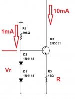
A simple CCS is arranged the following way:
- take a voltage reference Vr, more than 1 x Vbe (2 diodes = 2 x Vbe = 1.4V will be OK; 1 Red LED = 1.8V will work as well);
- take NPN transistor;
- set your voltage reference between the CCS transistor's base and the negative rail;
- use a resistor R between the CCS transistor's emitter and the negative rail - that's the one, setting the CCS current, which is Iccs = (Vr - Vbe)/R;
- now you can convert the formula in a way that R = (Vr - Vbe)/Iccs; that's the way you find your R value.
See attached.
Now. Transistor power ratings. Many TO-92 devices will have maximum power of 500-600mW. But this is the maximum power, it stands WITH the best possible heatsink. Beyond that power it breaks. TO-92 is a very small package (and a small die inside it) - even 250mW have to go somewhere, so without any heatsink it will heat-up considerably. Even TO-126 at 10mA becomes pretty warm (well, I normally use higher rails, like +/-50V, but anyway).
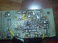
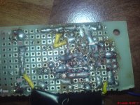
Soldering quality. There are lots of flux remains everywhere. I don't know what flux you use, but most of the liquid or paste ones conduct rather badly. Accept a simple rule - make the board clean and dry before you switch the power on. Otherwise many surprises may arise, very difficult to diagnose.
Hope that helps 😉
Cheers,
Valery
In normal operation, the current through those 22R resistors is roughly 12mA.
Simple calculation (P=I*I*R) gives us dissipation of 3.1mW on those resistors.
Even 1/8W will work fine there.
The point - it's far from normal operation...
OK - you asked for it.
Look at the way your dynamic load is organized (T10).
It's only partially dynamic (I would say - very slightly dynamic).
In fact, only 3.5mA from overall 10.7mA goes through T10.
The normal way of arranging the dynamic load is using a CCS.
A simple CCS is arranged the following way:
- take a voltage reference Vr, more than 1 x Vbe (2 diodes = 2 x Vbe = 1.4V will be OK; 1 Red LED = 1.8V will work as well);
- take NPN transistor;
- set your voltage reference between the CCS transistor's base and the negative rail;
- use a resistor R between the CCS transistor's emitter and the negative rail - that's the one, setting the CCS current, which is Iccs = (Vr - Vbe)/R;
- now you can convert the formula in a way that R = (Vr - Vbe)/Iccs; that's the way you find your R value.
See attached.
Now. Transistor power ratings. Many TO-92 devices will have maximum power of 500-600mW. But this is the maximum power, it stands WITH the best possible heatsink. Beyond that power it breaks. TO-92 is a very small package (and a small die inside it) - even 250mW have to go somewhere, so without any heatsink it will heat-up considerably. Even TO-126 at 10mA becomes pretty warm (well, I normally use higher rails, like +/-50V, but anyway).
Soldering quality. There are lots of flux remains everywhere. I don't know what flux you use, but most of the liquid or paste ones conduct rather badly. Accept a simple rule - make the board clean and dry before you switch the power on. Otherwise many surprises may arise, very difficult to diagnose.
Hope that helps 😉
Cheers,
Valery
Attachments
they wanted to lie me that i burn my last transistors. 🙂
you said "Look at the way your dynamic load is organized (T10)"
i am not using dynamic load since the local feedback (R2(two purposes)) lowers the distortion as dynamic load. i dont have good common sense about dynamic load.
im using T10 for another purpose, (if you drive lateral fets directly)(capacitance)
anyway thanks for the explaination.
i dont have smth to clear the flux.
😱 are u kidding with me ? is this some kind of joke ?
you said "Look at the way your dynamic load is organized (T10)"
i am not using dynamic load since the local feedback (R2(two purposes)) lowers the distortion as dynamic load. i dont have good common sense about dynamic load.
im using T10 for another purpose, (if you drive lateral fets directly)(capacitance)
anyway thanks for the explaination.
i dont have smth to clear the flux.
R4 sets that current at about 9-10 mA. Yes?
R2 sets Vbe of T3 at about 6.8V...if it could get there.
So actually most of the 9-10mA is going to be base current for T3
What is current gain of T3?
That is the current through 22R...more or less.
Close?
Added note: IMHO running something at 50% of rating better have some kind of heat sink.
😱 are u kidding with me ? is this some kind of joke ?
Last edited:
they wanted to lie me that i burn my last transistors. 🙂
i meant they wanted to plug it without the resistors.
what is the maximum Pd without heatsink ? 1/3, 1/4 ?
if you want dynamic load this is the way (the attachment), but,
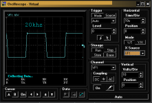
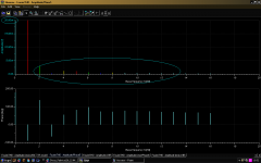
@ 20khz fft is worse than mine's fft (mine is beauty and H2 dominant). (uploaded fft is @1khz).
mine theory is that this current must'n be constant !
Attachments
this is the version i will use if 128mW is ok without heatsink 🙂
gives me THD 0.068% @ 20khz and perfect square.
WHat else ?
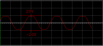
and this is the clipping @ 316mv rms
hhahah 😀
gives me THD 0.068% @ 20khz and perfect square.
WHat else ?
and this is the clipping @ 316mv rms
Hi JMFahey,
That big resistor, 1800KW, do you have SMD pcb connectors for it?
hhahah 😀
Attachments
Last edited:
it can be mounted directlyHi JMFahey,
That big resistor, 1800KW, do you have SMD pcb connectors for it?
Last edited:
i meant they wanted to plug it without the resistors.
Those resistors are normally used not to protect something - they are parts of the simple RC filter, used to decrease the rails ripple for the front-end.
what is the maximum Pd without heatsink ? 1/3, 1/4 ?
Stick for 1/4 or less - more or less safe for now.
In some cases, if no thermo-compensated references used to set the operating points - even if the transistor is barely warm, a small local heatsink is recommended in order to stabilise its operating point.
if you want dynamic load this is the way (the attachment), but,
@ 20khz fft is worse than mine's fft (mine is beauty and H2 dominant). (uploaded fft is @1khz).
This is not a dynamic load. Can you see the difference of what I have attached to my previous post and what you have attached to your previous post? Nothing close to dynamic load. The structure on your schematic does not make sense at all - what's the reason of having emitter of T10 connected to the front-end output. The result is the opposite to what you are trying to achieve.
mine theory is that this current must'n be constant !
This is the wrong theory 🙁
Unless it's a push-pull, driven from the both ends, or current-mirrored.
But let's stop here for now - at this stage, just take as granted, that the true dynamic load will give you much less distortion than any reasonable resistive one.
yes, this is the reason im using them, i said that they tried to convice me that these 22r must be powerful ones and this would let me try without them, but i know they are perfect and if i try without them my bc560 will blow instantly, i mentioned i dont have another right now.Those resistors are normally used not to protect something - they are parts of the simple RC filter, used to decrease the rails ripple for the front-end.
ok im using 128mW now look at my post #17, this is the sch im gonna use.Stick for 1/4 or less - more or less safe for now.
ok, the reason to use emitter to output i mentioned is for better handling capacitive load.This is not a dynamic load. Can you see the difference of what I have attached to my previous post and what you have attached to your previous post? Nothing close to dynamic load. The structure on your schematic does not make sense at all - what's the reason of having emitter of T10 connected to the front-end output. The result is the opposite to what you are trying to achieve.
Why ? mine way shows better results.This is the wrong theory 🙁
In a simple class A stage there are resistor, not CCS. I know what is the mechanism but think its a trap.
- Status
- Not open for further replies.
- Home
- Amplifiers
- Solid State
- hepl me please, need fast help