I built a blameless amp based on a PCB from Jim's audio, but have been doing some tweaking to some component values. Mostly due to VAS problems relating to CCS. The rise time was really poor from the beginning, so I wanted to improve that, and it did not seem stable at transients. Also transients were carried over to the IPS CCS as it was.
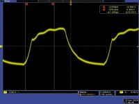
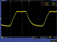
I see ringing on the current of Q7 collector, and I think this is the root of my problem.
I tried replacing the VAS CCS with a resistor in sim, and then the square wave is super clean. Real life is worse than the simulation, and I see a significant change in the waveform when touching Q7 (VAS CCS). (see scope pics)
I plan to change the compensation later, but as it is now, it's standard miller.
Hope somebody has some easy fix for my problem 🙂
Attachments
The standard experiments which people perform in situations like yours, are
1. Increase R6 to 10K and test the circuit
2. Reduce R6 to original value; add a 10,000 pF (10 nF ; 0.01 uF) capacitor between base and collector of Q4 and test the circuit again
Also I recommend that you ask the simulator: "What is the DC bias current in resistor R7? Is it really 2.6mA as someone wrote on the schematic?"
100 pF base-collector Q7? Resistor 10k from collector Q7,Q9 to ground and capacitor 200-470 pF in parallel (or to the bus).
Member
Joined 2009
Paid Member
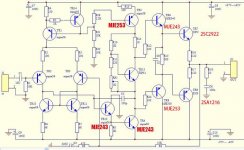
I believe the connections around R33 are incorrect as well. The base of the upper driver should be connected after it, not before
The value of R32 is too small. It should be at least 1K - this prevents the VAS CCS robbing all of the bias voltage from the LTP if the amplifier is driven into clipping
MJE340/350 make rubbish drivers. Try MJE243/253
The value of R32 is too small. It should be at least 1K - this prevents the VAS CCS robbing all of the bias voltage from the LTP if the amplifier is driven into clipping
MJE340/350 make rubbish drivers. Try MJE243/253
Last edited:
Member
Joined 2009
Paid Member
fT 10 times to short
That may be not significant if you use these in the driver stage - I have used them accordingly.
The mistake here is to use them in the Vas - a Vceo of 300 does not put an MJE340 at the top of the list of desirable attributes.
The relevant specification is the Gain Bandwidth product of the circuit and for this device fT is important. The latter information on this is absent in the datasheet but some sources put that at 10MHz - not enough starting capital.
There are better suited small signal transistors for use as Q10, and Q9 which will allow higher aim points.
As rough approximation re 10MHz, this has be divided by 20 for the closed loop gain and multiplied by 0.707 to allow at the -3dB frequency point where-ever that lies.
In a race to the bottom line of unity, phase will always get to -180 degrees first without any compensation.
Phase shift is more rapid than decline in gain and starts to change a decade in frequency in advance of the frequency point where gain is down to 70%.
Thank you for all the replies!
Self wrote about improving slew rate in his book, and mentions capacitance between base and emitter of Q7 as a problem, so I simulated this before and found decreasing R13,R14,R32 improved things a bit.
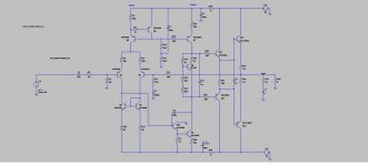
As you see in the attached original schematic, the 340/350 were replaced as suggested, but since that is what I could get locally, I went with them. I have a few 649/669 that I could try if you think those are better? However, I have not seen any real stability improvements in simulations when trying other transistors. I guess changing these would allow better OLBW, but for now I would only like to get better stability in the VAS.
I did as Mark suggested in the simulation, but did not see much improvement, and I can't do it on the amp right now since I don't have the capacitors.
I am a bit reluctant to add caps too (to rail or ground), since I don't know how it will affect PSRR. The PCB has no RC filtering on the rails for the small signal part of the amp either, making things worse I would guess.
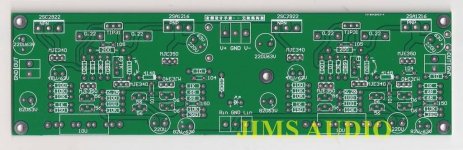
EDIT: as seen, the actual PCB markings does not really correspond to the schematic either.
Self wrote about improving slew rate in his book, and mentions capacitance between base and emitter of Q7 as a problem, so I simulated this before and found decreasing R13,R14,R32 improved things a bit.
As you see in the attached original schematic, the 340/350 were replaced as suggested, but since that is what I could get locally, I went with them. I have a few 649/669 that I could try if you think those are better? However, I have not seen any real stability improvements in simulations when trying other transistors. I guess changing these would allow better OLBW, but for now I would only like to get better stability in the VAS.
I did as Mark suggested in the simulation, but did not see much improvement, and I can't do it on the amp right now since I don't have the capacitors.
I am a bit reluctant to add caps too (to rail or ground), since I don't know how it will affect PSRR. The PCB has no RC filtering on the rails for the small signal part of the amp either, making things worse I would guess.
EDIT: as seen, the actual PCB markings does not really correspond to the schematic either.
Attachments
Last edited:
I replaced Q7 with a 2SB649, and it improved it a bit. I would say it's almost acceptable now.
however, looking at 1kHz distortion now, it is high with 2nd at abt -70dB left, and -80 right channel. Higher order harmonics are on a downwards slope. Stays the same without load, so from what I understand, it should not be from the output stage. I have to go back to simulation I guess.
however, looking at 1kHz distortion now, it is high with 2nd at abt -70dB left, and -80 right channel. Higher order harmonics are on a downwards slope. Stays the same without load, so from what I understand, it should not be from the output stage. I have to go back to simulation I guess.
Ok, distortion problem solved. It turned out that running one channel with load while measuring the other without load caused a problem. Some kind of crosstalk on the PCB. I added resistors to RC-filter the supplies to IPS and VAS, and the distortion in now looking quite nice with 2nd harmonic at abt -90dB, and not much variation depending on load.
I have looked in to the VAS transistors a bit (Q7, Q9, Q10), and I would like to try some faster devices here. I don't have any lying around that would work, mainly because the pcb layout is for ECB pinout, and I have only CBE. I would like to avoid crossing pins. I guess they should be rated at least 80V since I plan on running dual 40V supply. They should also be easy to source in Europe. I think low Cob would be nice to try especially for Q7?
I hope somebody has suggestions?
Last edited:
One of the problems you have with medium power transistors in the Vas is the chip area has to be proportionately larger than it would be with a small signal transistor.
As the result of this the capacitance between the layers - particularly the collector and base is also larger.
This capacitance is non-linear and in a common emitter amplifier stage the remedy is to swamp this with an external capacitor that is linear in parallel.
A common emitter amplifier i.e. one with a load in the collector connection will amplify whatever capacitance there is in the feedback path from the collector to base.
In an ECB package a BF469 has an fT of 100MHz or you could look for a 2SC or KSC prefix device.
Small signal transistors (TO-92) should be ok too I guess to keep capacitance down?
Or are there none of those with the correct pin-out (collector as center pin) and specs? Maybe I have to swap the legs anyway if that's the case (most of the ones I have are used and the legs are cut).
Thank you for your help, and sorry about the newbie questions..
Or are there none of those with the correct pin-out (collector as center pin) and specs? Maybe I have to swap the legs anyway if that's the case (most of the ones I have are used and the legs are cut).
Thank you for your help, and sorry about the newbie questions..
Single core colored conductors from a computer network cable will help solve the problem with the leads 🙂
I found these TO-92 at the local supplier that seem to have the collector in the middle, and ft around 100MHz. The BC6xx seem to be capable of some current and pretty linear beta with current too, not sure how relevant that is in this application though?
PNP (Q7 CCS)
BC640
KTA1023
NPN (Q9, Q10)
BC639
No/maybe/ok ? 🙂
PNP (Q7 CCS)
BC640
KTA1023
NPN (Q9, Q10)
BC639
No/maybe/ok ? 🙂
I was about to post to suggest BC639 for the Vas. Fine that your local supplier has this and BC640.
Your simulation shows voltage rails that sit at +/- 36V and I would suggest you stick with this.
BC639 and BC640 max Vceo is 80V with +/- 40 volt rails with supply regulation and variations in your mains voltage that is not so safe.
BC639 and BC640 max Vceo is 80V with +/- 40 volt rails with supply regulation and variations in your mains voltage that is not so safe.
If you can't source low capacitance high voltage transistors, a cascoded VAS and its load would be an approach.
Use a low voltage low capacitance device to drive your MJE340/350 as cascode stages.
For +/-40 supply, 100+V devices seem reasonable, 80V devices do not. "Absolute maximum" is not a place to sight-see, its a place to avoid 🙂 Anyway MJE340/350 are not an issue for this.
Use a low voltage low capacitance device to drive your MJE340/350 as cascode stages.
For +/-40 supply, 100+V devices seem reasonable, 80V devices do not. "Absolute maximum" is not a place to sight-see, its a place to avoid 🙂 Anyway MJE340/350 are not an issue for this.
@Rallyfinnen,
KTA1023 provided your supplier also stocks the complement KTA1027 you should go with these - for Vceo and fT.
These should also be less susceptible to Early Effect. In that regard if you can find .models look up VAF to see how high this is in comparison to low voltage transistors.
KTA1023 provided your supplier also stocks the complement KTA1027 you should go with these - for Vceo and fT.
These should also be less susceptible to Early Effect. In that regard if you can find .models look up VAF to see how high this is in comparison to low voltage transistors.
Thank you for all for educating me 🙂
I looked at the 80V too, but I'm not sure what supply I will use it with. Iq will probably be on the higher side (because I like it, and Re is low), so I don't want to go too high on the supply voltage anyway. I will have to use something within the limits I guess. This is just a 'fun build' to learn, I'm trying to re-use some output devices and other stuff I have lying around. Hopefully it will sound nice too.
The supplier did not have the KTA1027, so I never ordered those. They were a bit expensive too, compared to the BC's.
- Home
- Amplifiers
- Solid State
- Help with VAS CCS stability on blameless amp?