Hi guys!
Ive made a pcb based on Jens Rasmussen`s Leach amp clone, since i wanted to be able to separate the board, i found i basically had to make a new pcb layout. While doing so, i changed a few of the tracks from topside to bottom side, but it seems like ive done some more errors, i keep blowing the fuse. If i detach wire connection from driver transistors to output board, the power usage sinks to a low level, so the error seems to be on the "input" board side...(Or?)
Could you have a look at this and tell me if you see something wrong? (pictures attached).
Thanks
Attachments
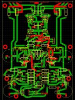
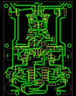
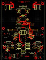
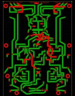
Looking at your pics I see already clearance problems between tracks and mounting holes, either it's just the small pic size or you didn't do a clearance check.
Otherwise there's not much we can do for you, you have to debug the board on your side. Means checking all voltages and currents and comparing to expected values.
A lot can go wrong when doing your own boards, that could be wrong part definitions (usually from downloaded other people's part libraries), to wrong routing (however, your program should check for that), wrong schematic, to a faulty produced board from the board house (happened to me once), to simpe miswiring...
Sorry, Hannes
Looking at your pics I see already clearance problems between tracks and mounting holes, either it's just the small pic size or you didn't do a clearance check.
Otherwise there's not much we can do for you, you have to debug the board on your side. Means checking all voltages and currents and comparing to expected values.
A lot can go wrong when doing your own boards, that could be wrong part definitions (usually from downloaded other people's part libraries), to wrong routing (however, your program should check for that), wrong schematic, to a faulty produced board from the board house (happened to me once), to simpe miswiring...
Sorry, Hannes
Hi Hannes!
Thank you for your reply.
Its a small picture, worst clearance is 0.3mm, and the printed plate is good there.
Im not sure if i can check for wrong routing in this program i use (Express PCB).. I Can link with schematic, but thats about it i believe.
Ive etched the board my self
Hi Hannes!
Im not sure if i can check for wrong routing in this program i use (Express PCB).. I Can link with schematic, but thats about it i believe.
Ive etched the board my self
You need to link it to the shcematic then check for errors.
My cad software checks in two ways, either an integrity check (compares sch and pcb) or simply do a forward annotate and look for changes.
Doesn't your cad package have a net and design rule check ? You should not use any pcb package unless it has these facilities otherwise you are asking for trouble 🙁
- Status
- Not open for further replies.