Hello all, I have been trying to repair one channel in a PA7II, and could really use some help. I have worked on other PA7 before (succesfully), but the fault in this one eludes me.. 😕
One channel is working fine, but the other has extreme negative DC offset, about 2V lower than the rail voltage!
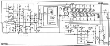
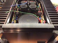
Please see attached schematic of input and VAS with test voltages noted, as well as complete schematic for one channel.
I have measured and tested all components, and only found one defective so far: ZD12 (3.2V zener).
But I have now also replaced the driver pair, and most of the TO92 transistors (Q106, Q107, Q108, Q109, Q110, Q111, Q112).
-Yes I know, I know... I did replace them one at a time though, and retested in between.
All resistors and caps test good.
I have also tried replacing the SK240 JET with a set of SK170 (real ones!), to rule out a leakage issue. No change, so the SK240 is back in.
All the outputs have been desoldered and tested out of circuit. At the moment I have just one set of outputs soldered in.
What am I missing? What can cause -40V (or -74 if run at full voltage) at the Collectors of both Q110 and Q112? - where it should be +2V and -2V.
Thanks in advance!
One channel is working fine, but the other has extreme negative DC offset, about 2V lower than the rail voltage!
Please see attached schematic of input and VAS with test voltages noted, as well as complete schematic for one channel.
I have measured and tested all components, and only found one defective so far: ZD12 (3.2V zener).
But I have now also replaced the driver pair, and most of the TO92 transistors (Q106, Q107, Q108, Q109, Q110, Q111, Q112).
-Yes I know, I know... I did replace them one at a time though, and retested in between.
All resistors and caps test good.
I have also tried replacing the SK240 JET with a set of SK170 (real ones!), to rule out a leakage issue. No change, so the SK240 is back in.
All the outputs have been desoldered and tested out of circuit. At the moment I have just one set of outputs soldered in.
What am I missing? What can cause -40V (or -74 if run at full voltage) at the Collectors of both Q110 and Q112? - where it should be +2V and -2V.
Thanks in advance!
Attachments
Seems that a circuit branch to the positive rail is open. Look for an open foil trace (or via).
Check each circuit node for having same voltage on each component that is connected to that node.
For example, the collector of Q102 and the base of Q108 should both have the same voltage.
Also the base and collector of Q103, the base of Q102, and the base of Q109 should all have the same voltage.
Any difference shows an open circuit in that node's connections.
Do this for all of the circuit nodes, marking each schematic component terminal with a red pen when checked.
Include the connectors, jumper wires, and vias as components in the checking.
Last edited:
Hi rayma, thanks, I will try that, and be meticulous about it. Will report back later this week..
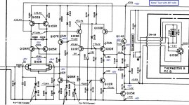
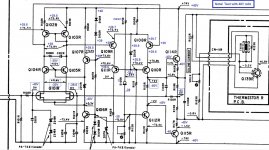
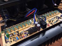
Hi, new picture attached with more measurement points...
I have checked all nodes for identical voltage. Have checked long traces for continuity and closely inspected the PCB. I can't find any defects there.
When I rechecked resistors, R115 gave some "funny" results, so I replaced it - seems to be intermittent - going open. That didn't solve the larger issue though.
I am starting to suspect D105, whch is an E-102 1mA CRD (is removed from PCB in the pictures). Semitec makes them, but they are backordered at Mouser.
Other than that, I am running out of things to try, so good ideas would be much appreciated 🙂
Attachments
Completely off-topic, but I admire the clever way the Vbe multiplier is mounted on a snap-off internal sub-pcb - or at least that appears how its done. Reduces assembly and testing overheads presumably.
I am starting to suspect D105, whch is an E-102 1mA CRD (is removed from PCB in the pictures). Semitec makes them, but they are backordered at Mouser.
Other than that, I am running out of things to try, so good ideas would be much appreciated 🙂
If you suspect it, try it in the working channel - 100% diagnosis or elimination 🙂
Repairs on amps with one working channel are always your handy backup when the problem is puzzling.
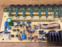
Mystery solved! and some pictures
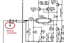
Hello, the "mystery" has been solved: The reason for the DC offset I was seeing, was that the input signal cable wasn't connected.
The circuit doesn't work properly without the input section being grounded, and this is done via the signal cable shield (see diagram pic) - which has to be disconnected during disassembly. What can I say... 😱
I did replace the D105 1mA CRD with two new 0.5mA CRD in parallel (these I could get from Mouser). This gave better voltages on the check points.
The other channel (right) that seemed to be working ok, turned out to be marginal upon closer inspection: It had high distortion and with unstable readings. Replacing Q110, Q111, Q112 and the driver pair solved these issues.
As substitute for SA1370/SC3467 I used KSA1381/KSC3503, which has very similar parameters, but is in TO126 package instead of TO92-Mod. The larger devices fit perfectly though, and I think the higher watt rating is good, as these are working relatively hard.
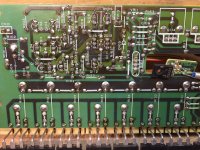
Also, both channels had many bad solder joints, and needed extensive reflowing. The PCBs are not very high quality (odd for such an otherwise solid amp), so care is required - especially when replacing components.
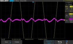
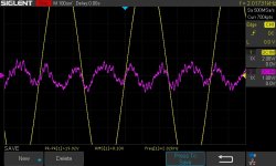
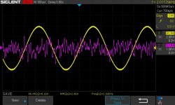
I have attached some pictures, including oscilloscope screens of distortion measurement using HP 339A.
The THD residual is seen together with the test signal (yellow). From 1w to 100w (8 ohm, 2 Khz sine) the THD is app. 0.01%, but harmonics looks cleaner at higher power levels, as seems typical for large amplifiers.
Thank you for your help!
Hello, the "mystery" has been solved: The reason for the DC offset I was seeing, was that the input signal cable wasn't connected.
The circuit doesn't work properly without the input section being grounded, and this is done via the signal cable shield (see diagram pic) - which has to be disconnected during disassembly. What can I say... 😱
I did replace the D105 1mA CRD with two new 0.5mA CRD in parallel (these I could get from Mouser). This gave better voltages on the check points.
The other channel (right) that seemed to be working ok, turned out to be marginal upon closer inspection: It had high distortion and with unstable readings. Replacing Q110, Q111, Q112 and the driver pair solved these issues.
As substitute for SA1370/SC3467 I used KSA1381/KSC3503, which has very similar parameters, but is in TO126 package instead of TO92-Mod. The larger devices fit perfectly though, and I think the higher watt rating is good, as these are working relatively hard.
Also, both channels had many bad solder joints, and needed extensive reflowing. The PCBs are not very high quality (odd for such an otherwise solid amp), so care is required - especially when replacing components.
I have attached some pictures, including oscilloscope screens of distortion measurement using HP 339A.
The THD residual is seen together with the test signal (yellow). From 1w to 100w (8 ohm, 2 Khz sine) the THD is app. 0.01%, but harmonics looks cleaner at higher power levels, as seems typical for large amplifiers.
Thank you for your help!
Attachments
- Home
- Amplifiers
- Solid State
- Help with Nakamichi PA7II repair