I have a problem with an ML-9 amplifier channel, and I need advice. One channel works fine, but the other doesn't. I have disconnected all output transistors, and although I am able to see an amplified input signal at the output of the second amplification stage (the input to the 7-diode array), the DC offset at that point should be about +2.25 volts; instead, it's 420mv. The voltage across the 7-diode array is 4.53 volts (0.42 volts at the top of the array and -4.11 at the bottom, for a total voltage drop of 4.53.) Because the DC offset is almost 2 volts more negative than it should be, the pre-amplified signal saturates when the input voltage level is increased beyond about 100 mv. So far, I have not been able to determine why the DC offset across the diode array is 2 volts more negative than it should be.
I bought this amp for a really great price because someone before me unsuccessfully tried to find the problem; several parts were replaced. As a result, there may be more than one problem layered on top of the original problem. I don't mind clipping component leads or circuit board etches, but removing transistors will be a last resort, given the difficulty of desoldering these components. I have lots of voltage measurements, and I'm happy to take more measurements or replace some of the components.
Thanks for your help.
Attachments
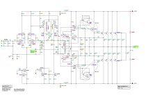
I’m assuming the “lollipop” next to the output and the one at the rightmost base on the LTP means that they’re connected as a global feedback loop? If that’s the case, removing the output transistors breaks the feedback loop and I wouldn’t trust any voltage readings. It looks like it has some kind of local feedback too, but I’d still be suspicious about any voltage I measure without the full loop in place.
Thanks so much! I'll reconnect those transistors and monitor the changes. By the way, the "lollipop" is a power transistor with a second transistor glued to the surface. I believe the purpose of these pairs is to provide heat compensation by adjusting the bias as the temperature rises. I think that may help prevent thermal runaway in the output stage.