I'm trying to layout a board for the old Jung AD744/AD811 design using Sprint-Layout 6.
After reading about the 811(or most high bandwidth op-amps in general) requiring an ideal board layout, I'm not sure how to go about designing a board for this relatively simple design.
For instance, I'm not sure whether or not to use a ground plane on the top or bottom of the board or the best way to deal with the signal and power grounds.
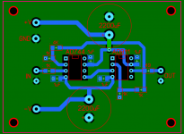
I started by trying to duplicate an old layout someone did back in the 90's as pictured below.
My plan is to use 1206 SMD caps at the supply pins instead of the larger through-hole caps in the pictured layout.
I'm also not against the idea of using 1206 resistors since they take up a lot less board real estate.
I've also attached the Sprint file(for the 90's design) I've been working on in case someone wants to change or totally redo what I have done. Please feel free to do so as I'm looking for different layout suggestions.
Thanks...
After reading about the 811(or most high bandwidth op-amps in general) requiring an ideal board layout, I'm not sure how to go about designing a board for this relatively simple design.
For instance, I'm not sure whether or not to use a ground plane on the top or bottom of the board or the best way to deal with the signal and power grounds.
I started by trying to duplicate an old layout someone did back in the 90's as pictured below.
My plan is to use 1206 SMD caps at the supply pins instead of the larger through-hole caps in the pictured layout.
I'm also not against the idea of using 1206 resistors since they take up a lot less board real estate.
I've also attached the Sprint file(for the 90's design) I've been working on in case someone wants to change or totally redo what I have done. Please feel free to do so as I'm looking for different layout suggestions.
Thanks...
Attachments
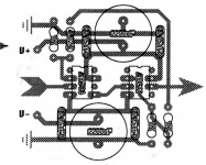
i still have my ad744+ad811 preamp from many years ago. i use it in between playing around with others. my layout is similar to what was done in The Audio Amateur several years back (i think the article is a free download), which is probably a little similar to your 1st post.
mine was done with a magic marker - it's a simple circuit.
so no CAD file to share.
mlloyd1
mine was done with a magic marker - it's a simple circuit.
so no CAD file to share.
mlloyd1
Hmm...93 views and no one has any layout examples their willing to share or any other suggestions?
I thought there were some folks here that are really good with PCB design software whether it be Eagle, Sprint or whatever.
Perhaps I posted in the wrong section.
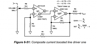
I've used hundreds of AD811s in high definition telecines but never as a hybrid amplifier. I CAN tell you a 4 layer board with a ground plane is quieter and more stable. Being a current feedback amp, the bandwidth is determined by R3 but don't fret, that's up in the 10s of MHertz. Directly beneath the amp I'd put a .2" x.2" hole in the ground plane to keep the capacitance lower particularly on the '-' input. They're flat as a pancake beyond 30 MHz. They also require GOOD bypassing which is always better with a ground plane.
G²
I'm sure a 4 layer board would be better, but I'm trying to suffice with a 2 layer board.
Instead of the .2"x.2" hole, is it not better to remove the ground plane from around all of the IC's pins to reduce capacitance?
Should the ground plane be on the top or bottom side of the board?
Instead of the .2"x.2" hole, is it not better to remove the ground plane from around all of the IC's pins to reduce capacitance?
Should the ground plane be on the top or bottom side of the board?
I use via-in-pad. All over the place. I only do small numbers of boards and I figure I can fix any soldering problems by hand if necessary. Not that there have been any, despite using a toaster oven for reflow.
It's often advised that removing the ground plane in the area of the opamp active pins and feedback circuitry can be helpful.
Make your tracks as wide as smallest pin they contact.
Use SMT caps. And opamps, for that matter.
You can only guess how effective the measures you have taken are, unless you have good test gear, but it's probably sufficient to get down to the measurement floor of a good soundcard + RMAA
Last edited:
My plan is to use 1206 SMD caps at the supply pins instead of the larger through-hole caps in the pictured layout.
I'm also not against the idea of using 1206 resistors since they take up a lot less board real estate.
If you want to do a first class job on the layout, use all smt parts on top, and a solid ground plane on the bottom..
Marce, my initial idea was to put the ground plane on top, with all traces and 1206 decoupling caps on the bottom of the board.
The vias on the SMD pads would connect those pads to the ground plane on top.
No, just the opposite, and use smt packages.
If you want to do a first class job on the layout, use all smt parts on top, and a solid ground plane on the bottom..
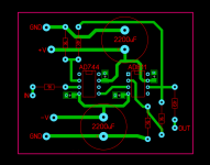
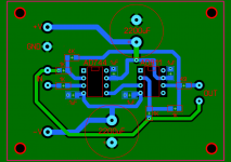
OK, here is my first attempt with all SMD parts(except for the 2200uF caps) and the ground plane on the bottom of the board.
Everything in blue is on top of the board and green is on the bottom side.
I realize I can reduce the width of the board on the left side, but at this point I'm more interested in getting the layout correct.
Does this look any better?
Thanks...
Attachments
My suggestion is not to share duty between signal ground and power ground - keep them separate and only joined at one spot. This in my experience gives the best subjective results.
I fully understand what you're saying, but I have no idea exactly how to do this here.
Perhaps if you can post a photo actually showing me how to "separate" the grounds and connect at them at only one point on this example, I'll be glad to implement it.
For me "seeing is believing".
")
Thanks...
You can get this much smaller. Use SMD opamp packages. Put them in line astern (or ahead). One will consume more current than the other (the output). Put it closest to the power inlet. Put the input at the other end of the input opamp. Arrange the feedback components absolutely as close to the pins as possible. Take the output ground to a spur between the principal smoothing caps at the power inlet. You can put big electrolytics on the bottom of the board. Don't be afraid to run the principal ground right under the opamps, many have grounded central pads for heatsinking. Put exclusion zones around the feedback components and associated pins. Floodfill both sides noting all ground returns and modifying to ensure no crossing is taking place and that in general return currents join the flow in order of magnitude.
Too lazy to draw you a sketch but I'll describe it in words.
Your schematic in post 1 shows three connections to signal ground (white triangle symbol) - they are the input volume pot, R2 amd R4. These nodes should have their own net, then that net goes to a single point on the power ground net.
Your initial layout, like your most recent one doesn't distinguish between signal and power grounds but lumps them all together. To me that's like not distinguishing between waste water and sewage but lumping them both together.
You can get this much smaller. Use SMD opamp packages. Put them in line astern (or ahead). One will consume more current than the other (the output). Put it closest to the power inlet. Put the input at the other end of the input opamp. Arrange the feedback components absolutely as close to the pins as possible. Take the output ground to a spur between the principal smoothing caps at the power inlet. You can put big electrolytics on the bottom of the board. Don't be afraid to run the principal ground right under the opamps, many have grounded central pads for heatsinking. Put exclusion zones around the feedback components and associated pins. Floodfill both sides noting all ground returns and modifying to ensure no crossing is taking place and that in general return currents join the flow in order of magnitude.
While I appreciate your suggestions, I'm not trying to see "just how small we can make this simple circuit" by using SMD op-amps.
As for all the other suggestions about putting the op-amps in "line astern", taking the "output ground to a spur", "putting the electrolytics on the bottom of the board", "running primary ground under the op-amps", "floodfilling both sides", I am totally confused as to what you're even talking about.
I'm by no means a PCB guru, that's why I'm trying to learn.
It's always MUCH easier to put things into words than it is to actually show someone the points you're trying to get across.
Too lazy to draw you a sketch but I'll describe it in words.
Your schematic in post 1 shows three connections to signal ground (white triangle symbol) - they are the input volume pot, R2 amd R4. These nodes should have their own net, then that net goes to a single point on the power ground net.
Your initial layout, like your most recent one doesn't distinguish between signal and power grounds but lumps them all together. To me that's like not distinguishing between waste water and sewage but lumping them both together.
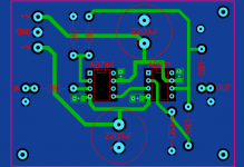
Is this what you're talking about? There is no volume pot on the board.
Signal grounds connecting to ground on the lower 2200uF cap only.
Attachments
- Status
- This old topic is closed. If you want to reopen this topic, contact a moderator using the "Report Post" button.
- Home
- Source & Line
- Analog Line Level
- Help with Jung AD744/811 PCB Layout