Good to know you sorted the oscillation problem.
Some points to note: the input stage is run at approximately 1mA (using a 12k tail resistor). If the currents in the input pair were equal (but I'm not sure they are), that would make them 500uA each. The slew rate of 0.5mA with a 220pF Miller capacitor is in the order of 2MV/s. A 20kHz sinewave at 8V is about 1MV/s, so I suspect the 20kHz performance will not be brilliant, which is a bit of a disservice to the high frequency output devices!
To improve the slew rate, it would be better to use emitter degeneration resistors, and a smaller capacitor. Perhaps 80kHz would be enough for a guitar amplifier - I doubt many valve amplifiers would be that good. So we are looking to reduce the Miller capacitance by a factor of about 4 and 47pF would be suitable. To keep the same frequency response the input stage gain should be reduced by 4 times, and that would require emitter resistors of 150 ohms. To balance the currents, the base resistor of the VAS transistor should be about 1.3 to 1.5k rather than 1k.
I would suggest using a 10k tail resistor rather than 12k; the currents could be increased but a CCS would be preferred if the resistance drops much below 10k.
The audio test with 4 ohm speakers was successful. Sounds great.
I'm using a 8.2k tail resistor. This lets me lower the supply voltage to 20 Vdc, even lower.
Also, input transistor Ic current is around 0.65 mA (the other is just over 0.7 mA; this values, as simulated in LTSpice).
I'm not sure how to simulate slew rate. I just placed a pulse generator, 50uS period, 16V swing, and measure the time that the signal at the VAS stage taked to reach its tfinal value. I attached the simulation. Please correct me if I'm wrong.
I will try lowering the Miller cap to 100 pF, just to get some more margin.
john_ellis, the emitter degeneration is for reducing the gain only? or does it have any other purpose?
AndrewT, I'll take note of that test, and will perform it next time.
Mooly, very interesting thread. I think that most of the time I'd be happy with just 5W of power, even though I like to get decent volume.
My tube amplifiers are between 6 and 12W, and I never push them to their limit (not the 12W one, at least).
Attachments
Pretty much the sole purpose of emitter degeneration in Miller compensated amplifiers is to address the slew rate. But effects of degeneration include (1) linearising the input impedance and response over a wider range (this is the main solution to slew rate limiting issues) (2) reducing distortion and (3) potentially increasing the frequency response. They also help to balance the emitter currents. Gain loss is a consequence of the local feedback. This form of local feedback can be used to control open loop gain and phase, and designers may exploit this not just in Miller compensation designs.
Local feedback resistors are also recommended in current mirrors using discrete transistors. (You might not need them in I.C. designs where the transistors are right next to each other and thus thermally connected about as closely as one can get.)
Local feedback resistors are also recommended in current mirrors using discrete transistors. (You might not need them in I.C. designs where the transistors are right next to each other and thus thermally connected about as closely as one can get.)
Mooly, now I'm going to solder this nice little amp on pre-perforated boards. I'm too lazy to design a PCB right now (though I probably will do sometime).
john_ellis, got it. Right now I'll probably just build this simple one, to free my protoboard for other circuits, but I'd like to experiment in a near future.
The audio session today with my good speakers by far excedeed my expectations.
According to simulation, I'm having about 3 V/us slew rate, which should be fine.
But the raise time is faster than the falling time.You can see in my last post's attachment.
It seems one output transistor is conducting harder than the other, as shown in LTSpice. This seems to happend with a sine input too.
I can't find the reason... do you know why??
Attachments
Pretty much the sole purpose of emitter degeneration in [Blameless-style 3 stage amplifiers having an LTP-IPS, a VAS, and a unity gain OPS] Miller compensated amplifiers is to address the slew rate. But effects of degeneration include (1) linearising the input impedance and response over a wider range (this is the main solution to slew rate limiting issues) (2) reducing distortion and (3) potentially increasing the frequency response.
The circuit designer seeks to independently control (i.e. to set) three performance parameters: (i) the unity gain crossover frequency, sometimes called "GBW"; (ii) the slew rate; (iii) the frequency of the right halfplane zero.
Fortunately, s/he has four design variables or "knobs" that can be adjusted and tuned, which work together to set the three performance parameters. The design knobs are: (i) the tail current of the LTP-IPS; (ii) the transconductance (gm) of the IPS; (iii) the value of the compensation capacitor, in picofarads; (iv) the transconductance (gm) of the VAS.
Because the number of knobs exceeds the number of performance parameters, more than one solution exists which meets all three design goals. Maybe an underappreciated facet of the circuit designer's art, is to add a (personalized) fourth design constraint/goal/rule-of-thumb, which steers the knob settings towards a single and unique solution, a solution that represents the designer's personal opinions about what is more important and what is less important.
Elerion - asymmetrical slew is probably due to imbalance in the diff pair transistor currents. The input pair operate at a lower current than the VAS so these limit the current that can charge/discharge the Miller capacitor. That was why I suggested you optimise the base resistor of the VAS to equalise them, but if you're happy with the circuit and don't need a better slew, perhaps it is OK for you.
On your slew rate...
In your attached sim you have the amplitude of the voltage source set to 16 volts pk/pk 🙂eek🙂.
Anyway, I got around 6 volt/uS but I'm using different models for the BD135/6 so not sure that makes a difference or not. And a much lower applied input voltage.
In your attached sim you have the amplitude of the voltage source set to 16 volts pk/pk 🙂eek🙂.
Anyway, I got around 6 volt/uS but I'm using different models for the BD135/6 so not sure that makes a difference or not. And a much lower applied input voltage.
Attachments
Oh, that was it.
If I use a smaller input, the slew rate is the same in both directions. About 6.5 V/us
Thanks Mooly. Could you share your discrete models file?
john_ellis, I think I managed to balanced the LPT quite well.
Please, look at the attachment, tell me if I'm wrong.
The VAS current is much higher though (~3.5mA).
Is it recommended that LTP current is close to VAS current?
Or maybe I didn't understand what you tried to tell me.
Mark Johnson, thank you for the additional info!
Attachments

You might find this of interest. It was a Practical Wireless design from the late 1970's and has a couple of unusual features.
a/ A soft start (upper left transistors)
b/ A really odd darlington arrangement on one side of the LTP.
c/ The VAS uses a bootstrapped arrangement making use of the output coupling cap. A neat idea and saves a capacitor.
I built this as a youngster and it sounded really good as I recall. It would probably translate to a lower supply voltage.
Attachments
Slew rate is controlled by the available current to charge or discharge the Miller capacitor (in this design). Since the charging and discharging is limited by the input transistor currents, that is what is giving the relatively slow response. Depending on which way you consider the capacitor, charging (say) is when the input device is fully on, then the available current is the LTP current less whatever the bias resistor shunts; then on the discharge the capacitor can only dump current through the bias resistor.
As the VAS can handle higher currents that tends not to be the Miller limitation (see below). The main concern is that during slew rate limiting, the LTP transistors are on or off, and then cannot amplify any signals.
The bias resistor on the VAS is not ideal because the Vbe of the VAS is not constant; so it's a balancing act. A current mirror is better, but not necessarily needed in your simple low power circuit - that would be taking it a step up the hifi ladder.
For illustration, I simulated your original (no degen resistors, 220pF) and for 8 to 8V peak swing get 2.3 and 2.8MV/s, for a 20kHz square wave input. If you use extreme degen (1k resistors) and reduce the capacitor to 10pF the input stage is almost free of cutting out (the LTP current could usefully be increased) but the slew rate is 22MV/s.
However, the next problem is the VAS current. If the current in the input stage devices changes by a significant amount (and even with 1k resistors they almost swing between 2x idling and cut off) the VAS may then cut out too. Usually it needs more current than the usual 4 to 6mA to avoid, but that depends on what choices you make: how fast you want the amplifier, whether the bandwidth is to be limited with an input filter, whether you degen the VAS ...
There are indeed many choices to be made...
Last edited:
Yes, Mooly, that circuit does look interesting. I've never seen a bootstrap like this one.
I don't understand what/why is the tap to C6/R11 to the input via a resistor.
john_ellis, I've been playing with degeneration and now I better understand how it influences slew rate.
What do you mean by "input stage devices [...] almost swing between 2x idling and cut off"
The input stage for 3W output swings about 170 uA, while the idle input transistor current is in the order of 650 uA.
As I understand so far, how fast you want the amplifier depends JUST on the slew rate, and thus, input transistor max current and Miller capacitance; improved by emitter degeneration.
What direct consecuence would have increasing the VAS current? and degenerating it?
Yes, Mooly, that circuit does look interesting. I've never seen a bootstrap like this one.
I don't understand what/why is the tap to C6/R11 to the input via a resistor.
It raises the input impedance as it is a form of bootstrap in itself. Without the cap and the input impedance is around 180k. Add the cap and that goes to nearer 5 meg ohm. All measured at 1kHz.
If you really want to reduce the Miller effect, you want a cascode.
http://www.seas.upenn.edu/~ese319/Lecture_Notes/Lec_11_Miller_Effect_08.pdf
http://www.seas.upenn.edu/~ese319/Lecture_Notes/Lec_11_Miller_Effect_08.pdf
Yes if the collector-base capacitance is dominant, but in Miller compensated amplifiers it is usually the capacitor which is dominant (Self calls this Cdom). For this case a cascode will not help.
What cascode stages are usually used for is to eliminate Early effect distortion
What cascode stages are usually used for is to eliminate Early effect distortion
Elerion - I just mean that in a diff amp, each transistor should conduct half the tail current (preferably exactly). Therefore the maximum swing either transistor can see is a current 2x its idling value or cut off.
In a normally working amplifier the current excursions are small - the smaller, the better for lower distortion, so the normal swing would usually be designed to say +/-10% (the diff amp. itself provides a degree of second harmonic cancellation), but this depends on the design goals etc.
In slew rate limiting, the problem is that the transistors are pushed to their limits: one is cut off and the other conducting the full tail current or 2x its normal value.
Regarding the VAS current - this is a matter for evaluation and whether a design meets its goals, really. But generally, every time I've looked at the VAS currents in simulation the usual values can lead to cut-off (under extreme conditions I have to say), and higher VAS currents are able to avoid this, but it all depends on the other parts of the circuit.
Degeneration in the VAS can increase linearity [depending on the base drive: if current driven, gain linearity is already better than voltage drive (as that gives exponential response)], will improve the frequency response (or reduce the phase shift at a given frequency perhaps) and reduce Early effect distortion. Whether this is useful is once again dependent on the whole amplifier architecture, but even low values (like Self's 10 ohms in the Blameless) can help a bit.
Much more clear now. Thanks.
Today I tried LTP emitter degeneration (just 10 and 100 ohms), but it seems to worsens the slew rate a little bit (on real circuit; seems so in the simulation, by a quick test I've just done).
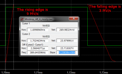
On the real circuit, with no emitter degeneration of any kind, and with 100 pF Miller cap, I get 5.5 MV/s. Wit degeneration, the raise and fall slows at the end.
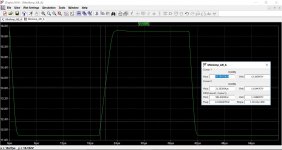
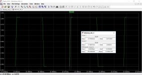
I need a 1uf cap between the drivers emitter (parallel to that 220 ohm resistor), or I get HF oscillations superimposed to the wave.
Also removing the Miller cap leads instantaneously to oscillations (this, expected).
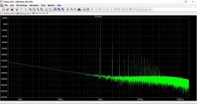
Harmonic content is so much different from simulation. Contradicting the simulation, I get primary 2nd harmonic, just -30 dB below the fundamental. Third and higher harmonics are much much lower, probably more or less at the level shown in the simulation, around -50 dB. At similar output power, of course.
I did some tests with a good speaker and some music of different styles, and it really sounds nice. Nothing I can blame,... at low power, so far.
Today I tried LTP emitter degeneration (just 10 and 100 ohms), but it seems to worsens the slew rate a little bit (on real circuit; seems so in the simulation, by a quick test I've just done).
On the real circuit, with no emitter degeneration of any kind, and with 100 pF Miller cap, I get 5.5 MV/s. Wit degeneration, the raise and fall slows at the end.
I need a 1uf cap between the drivers emitter (parallel to that 220 ohm resistor), or I get HF oscillations superimposed to the wave.
Also removing the Miller cap leads instantaneously to oscillations (this, expected).
Harmonic content is so much different from simulation. Contradicting the simulation, I get primary 2nd harmonic, just -30 dB below the fundamental. Third and higher harmonics are much much lower, probably more or less at the level shown in the simulation, around -50 dB. At similar output power, of course.
I did some tests with a good speaker and some music of different styles, and it really sounds nice. Nothing I can blame,... at low power, so far.
Degenerating the input stage without changing the Miller capacitor will degrade the slew rate. That is the point: you can reduce the capacitance after adding the emitter resistors and still maintain bandwidth. See graphs.
Higher second harmonic: could be due to wiring! Check where you connect the feedback resistor. It should be to the wire from the output side (to the output capacitor), not before as differences in resistance between NPN and PNP output connections may cause the imbalance.
Or related to the wiring on the decoupling capacitor(s) again.
Getting the design right is one thing; getting the layout to behave is another which we all have learned.
Attachments

- Status
- Not open for further replies.
- Home
- Amplifiers
- Solid State
- Help with design for a simple low power audio amplifier