Hi, i'm pretty new to solid-state, and need a little help.
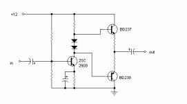
I've got some new transistors, and im not exactly sure how to bias this design, ive drawn.. so i dont know the resistor values..
first, here are datasheets for the transistors:
2SC2909
http://service.semic.sanyo.co.jp/semi/ds_pdf_e/2SC2909.pdf
BD237 & BD238
http://www.onsemi.com/pub/Collateral/BD237-D.PDF
I'd prefer to use single 12v power supply, but this will probably not have much power out. I guess I could make a split rail ±25v power supply, and that would eliminate the output capacitor as well.
also, should i implement some type of feedback? duo suggested it is needed..
I'm just toying with transistors for now, so this isnt exactly mission critical..
Attachments
> <i>I've got some new transistors</i>
Design first, <b>then</b> figure out what transistors fit the needs.
> <i>I'd prefer to use single 12v power supply, but this will probably not have much power out. I guess I could make a split rail ±25v power supply, and that would eliminate the output capacitor as well.</i>
Use the capacitor. Bad things happen on the test bench; the cap protects your speaker. Anyway this topology really is no good for split rail supply.
12V will make 2 watts in 8 ohms. Not much, but often plenty. +/-25V makes a LOT more power, about 32 watts in 8 ohms. BUT a 25V rail driving an 8Ω speaker will give 25/8= 3 Amp peak current. Those BD237 transistors are only rated 2A current, and that's optimistic: their Hfe falls above 0.1-0.5 Amps so they get very hard to drive. Even a 12V supply and 8Ω is pushing them hard. See? Rough-out the design with imaginary transistors with generic parameters, see what parameters are critical, see if you can find transistors like that at a good price.
> <i>how to bias this design, ive drawn.. so i dont know the resistor values..</i>
Yes, basic transistor amp design has become a Lost Art.
First: ignore the emitter followers. Bias a 1-transistor voltage amp. If you get that working, adding the emitter followers is fairly easy.
Then <b>put part numbers on plans</b>, or it is almost impossible to cyber-talk about a circuit when we can't just point to the part we are discussing.
<img src="http://music-club.rutgers.edu/headfonz/Colt45-2.gif">
Amps usually work best when the plate or collector is biased to about half the supply voltage. So we hope to make the collector of Q1 end up at 6 volts.
We pick a collector current. For general use, 1 milliAmp is often a good value, and makes the math easy.
The voltage across R3, the collector resistor, is about 6 volts. The current in it is about 1mA. So we compute 6V/1mA= 6KΩ. Since we are pulling numbers out of a hat, if we have a 4.7K resistor in that hat it is close enough.
Now, how do we get 1mA to flow in Q1 and R3? We can apply 0.62 volts to the base.... except when the transistor warms up the current will soar to 10mA.
There are many ways to stabilize current. The simple way is an emitter resistor with a fairly large DC voltage drop. If this is our only bias stabilization, it should be much-much larger than the 30mV-60mV uncertainty in base-emitter voltage. In main cases, it should be large compared to the 0.6V B-E voltage, so supply variations do not matter too much. As a first-hack, 0.6V across the R4 emitter resistor and 10% of 12V, or 1.2V, at the Base is a good trial value.
With 1.2V at the base and about 0.6V base-emutter drop, the voltage on R4 is 0.6V. The same 1mA flows here, so it is 0.6V/1mA= 600Ω.
We want R1 R2 to give 1.2 volts. What impedance? Same as asking: What current? For generic transistors with Hfe of 100 or more, a safe trial value is to make the R1 R2 current about 1/10th of the collector current. Say 0.1mA. Then by inspection: R2=(12V-1.2V)/0.1mA= 108KΩ, R1=1.2V/0.1mA= 12KΩ.
Set that up. With any half-decent small-signal transistor (Hfe over 50, Vce over 12V, Ie(max) over 10mA), the collector will sit about half of the 12V supply and it will amplifiy linearly.
What is the gain? Assuming no load and zero-ohm source, it is roughly R3/R4 or about 10. The output impedance is essentially R3 or 6K. The imput impedance is about R1||R2||(R4*Hfe). Assuming Hfe=100, it is about 108,000||12,000||(600*100)= 9,152Ω. We can use 1µFd for C1 and get response down to 20Hz.
What if we use C2, emitter bypass? Now we need to know the intrinsic emitter impedance of the transistor. Easy: 26 ohms at 1mA. Or generally: 0.026V/Ie, where Ie is emitter current in Amps. That's theory; 0.03 works better in practice for real silicon transistors. 30/Ie is convenient for working in milliAmps.
Assuming that C2 has a much-much lower impedance than the emitter, the gain is now 6K/30 or about 200. That's rather high for one stage. Also the distortion will approach 25% before it clips, and over 2% at 1/10th that level. C2 has to bypass the 30Ω emitter impedance, so it will need to be around 330µFd. The input impedance is the same as before except with 30 ohms in the emitter: 108,000||12,000||(30*100)= 2,348Ωs. We need a 5µFd cap at the input; no, actually we probably want to double both C1 and C2 so their individual roll-offs fall well below 20Hz.
- Status
- Not open for further replies.