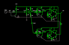
I'm having problems with the voltage gain stage on my amp. I'm using a BJTs like a CMOS inverter as the voltage gain, it works ok for high impedance loads, but has a problem driving low resistance. I've used a MOSFET as a unity gain buffer, but I'm losing 2-3 volts at the gate/source junction to turn the MOSFET on. Is there a better way to design this? I've tried using opamps as a buffer, but I would rather use discrete components.
Ryan
Ryan
Attachments
Uh, cmos is not a BJT bipolar junction transistor, it is MOS, metal oxide semiconductor.
The operating point of mos is so unstable with temperature (2 v to 5 v) I don't know of anybody that used them in class A commercially. I tried, vaccuum tubes are better. The gain of mos gate is outrageous, and I'm not sure tremendous feedback would work to stabilize the operating point for stable idle current. I tried & gave up with 2n7000 replacing an unobtainable EF86 tube.
Use a BD138/139 or MJE15028/29 for VAS like everybody else. There is a reason.
A few thoughts...
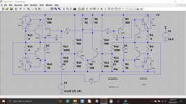
1/ The FET's in the power sections don't seem to have any bias arrangement. The gate is floating at DC.
2/ The driver sections using the NPN/PNP configuration (your CMOS buffer) look all wrong. In practice and with real device the transistors would just conduct uncontrollably. Use of 1meg and 300k resistors shows this is on a knife edge... even if the configuration was workable.
3/ Don't give up 🙂 Stuff like this is great to learn with.
Uh, cmos is not a BJT bipolar junction transistor, it is MOS, metal oxide semiconductor.
The operating point of mos is so unstable with temperature (2 v to 5 v) I don't know of anybody that used them in class A commercially. I tried, vaccuum tubes are better. The gain of mos gate is outrageous, and I'm not sure tremendous feedback would work to stabilize the operating point for stable idle current. I tried & gave up with 2n7000 replacing an unobtainable EF86 tube.
Use a BD138/139 or MJE15028/29 for VAS like everybody else. There is a reason.
Thanks - I use BC327/337 in the voltage gain stage. I think you may be confused on what I was asking. The voltage gain stage works, but only if it is connected to a high impedance load i.e. the MOSFET in the current stage. I was looking for a unity gain buffer to replace the MOSFET.
Thanks Mooly - I have finally gone with an op amp as the buffer and removed the MOSFET. As you said it does run hot, but it depends on the bias for the NPN/PNP drivers. I have alternated between cascaded diodes, LEDs, and a BC327 with resistors as shown. I've settled on the BC327 arrangement as it uses less power.
The op amp works okay at 20v - but I would like to increase the voltage/power and that is where the problem starts. I will begin to hit the threshold for current drain on the opamp... any suggestions?
The op amp works okay at 20v - but I would like to increase the voltage/power and that is where the problem starts. I will begin to hit the threshold for current drain on the opamp... any suggestions?
I would be looking at more conventional amplifier stages.
LTP front end with current source and current mirror.
VAS stage with capacitor feedback and current source.
Vbe multiplier.
Driver stage.
Output stage.
LTP front end with current source and current mirror.
VAS stage with capacitor feedback and current source.
Vbe multiplier.
Driver stage.
Output stage.
I can see what you are trying to do with this design but I see other problems as well. You are going to need the output stages to be wrapped around a tight feedback loop (opamp?) in order to control DC offset between the two halves. Remember in simulation all devices of the same type have 100% matching whereas real components do not.
Respectfully, to design an amplifier like any other electronic, mechanical or the like apparatus, doesn't consist in put some components or parts in a blender and give power to it. Continuing in such a way, will conduct to injuries and disappointment. I suggest to learn electronics basics before any attempt to design such a device, including simulations, because simulations are not real world conditions (only mathematical models) that not necessarily agree 100% to real world.
In other terns, before sitting in a car and start driving, is better to learn how this machine do its task. Otherwise you can finish crashed or severely damaged.
In other terns, before sitting in a car and start driving, is better to learn how this machine do its task. Otherwise you can finish crashed or severely damaged.
If you use LTspice (click my signature link) then there is quite a nice single rail example of an amp like you are trying to make.
Hmm, I think that LTC "PA amplifier" circuit is under "Educational" because it is so bad. The idea is that students are supposed to learn from all the mistakes and redesign it to correct all the problems. I had fun with it. I does include some cool examples of how to use SPICE.
Last edited:
Perhaps replace R5/R15 with a bootstrap and D1/2 with a Vbe multiplier it would sound even better
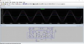
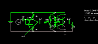
Actually - thanks for the help guys. I found a two transistor buffer design on angel fire that look promising. I've run it through the simulator and it seems to do the business. I'll give it a try on the breadboard this week. Cheers - Ryan

Update - I did some research of the last circuit, and the basis of the circuit is a Sziklai pair (thanks Wikipedia). if I replace the normal PNP/NPN in my voltage gain stage with their associates Sziklai pair, it improves the performance of the circuit. I don't need the MOSFET in the current stage and I can directly couple the voltage and current stages with a high value capacitor. It does run a bit hotter that than the original design, but that's a battle for another day. Thanks all - Cheers, Ryan
- Home
- Amplifiers
- Solid State
- Help my voltage gain stage in my amp