Reaching out for some assistance -
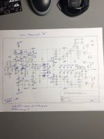
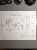
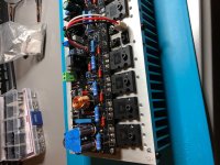
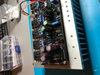
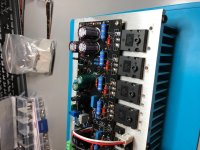
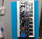
I recently built two channels of the Ampslab C300 by Michael Chua. I followed the build guide, schematic and write-up. Used 2N5551/5401 (Q1/Q2?Q3/Q4/Q5/Q6/Q7/Q8/Q9/Q13/Q14) for small signal transistors, 2SC3503e/1381e for the VAS (Q10/Q12) and bias sensing transistor (3503e) (Q11), MJE340/350 for drivers (Q15/Q16) and MJL4281a/4302a for outputs, using 0.47 emitter resistors instead of 0.39 on schematic.
Ironically the first channel, which I spent weeks carefully putting together has a lower gain then the second channel I put together in a weekend? I will call Channel "A" (marked as such in pictures) as the Low Gain channel and Channel "B" the Correct Gain channel. Channel 'A" has about 26 gain and Channel "B" has the correct 31 gain, according to the write-up information.
I have attached two identical schematics - one for each channel with DC voltages using a 40Vdc power supply with a DBT and one for each channel measuring AC voltages to try and trace down the issue. Which I am having trouble finding a smoking gun, so I'm here to ask for assistance. Tested with the same 0.056 input, I get 1.464 on low gain channel and 1.748 on the good channel
The only thing I have changed so far is Q10/Q12 (3502/1381) and matched using a cheap transistor tester so the Hfe and Vf were the same. Changed them because that's where the AC difference showed up first in the schematic as I was tracing voltages (this is my first time to try this process, so I'm sure I have missed a few keys probe points, but hoped what I have provided would give some direction.
I have tested all resistors and diodes (comparing schematic values and comparing to the "good" channel) - everything checked out in spec. or the same as the "good" channel if anything wasn't measuring to spec. I cannot see anything gravely wrong comparing either DC or AC voltages I measured. Triple checked R14/R15 (10k and 330r, respectively) with DMM, compare to working channel and confirm color codes, I believe these resistors set the gain - they both check out within 1%.
When tested with music - both channels had 15mV of bias (after 1 hour of idle warm-up) and offset was <5mV, they both play music without distortion, with the "low" gain channel about 5-6db lower volume (according to my Pre-amp volume control).
Thanks for any help getting this solved. Let me know if I can provide anything additional that will help find the issue.
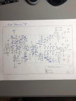
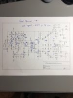
Attachments

I'm sure there is someone out there who can offer some ideas.
previous changes:
- changed out VAS transistors - NO CHANGE
what I've done since my first post:
Any ideas???!!! I'm thinking of changing R2 (10k) next, because something is drawing down the voltage there. R2 measures good with my DMM on the board, so I doubt that is the problem.
- I have also tried probing with a plastic pen to see if I have a bad solder joint, or loose connection anywhere - no amount of wiggling, jiggling or tapping seems to make any difference at that R1/C2 node, stays 0.048 (should be 0.058)

previous changes:
- changed out VAS transistors - NO CHANGE
what I've done since my first post:
- replaced all 2N5401/5551 after matching for Hfe with Chinese tester - NO CHANGE
- replace C1 (from 4.7uF film cap, to a 10uF bi-polar electrolytic cap (Nichicon) - NO CHANGE
- took more measurements and the node at R!/R2 has 0.058 Vac (same as input), but moving probe to node at R1/C2 voltage drops to 0.049Vac - on working channel there is no drop in voltage at R1/C2
- changed R1 (1k) to a 1% and tested resistor I removed and tests at 0.996r (perfect) - NO CHANGE
Any ideas???!!! I'm thinking of changing R2 (10k) next, because something is drawing down the voltage there. R2 measures good with my DMM on the board, so I doubt that is the problem.
- I have also tried probing with a plastic pen to see if I have a bad solder joint, or loose connection anywhere - no amount of wiggling, jiggling or tapping seems to make any difference at that R1/C2 node, stays 0.048 (should be 0.058)
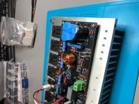
Problem SOLVED!!!
I can’t believe I did this but I put a 0.1uF cap in C2 instead of the 470pF it should have been. In my defense they are identical size, lead spacing and color, but it’s still these bad eyes I guess. I know I looked at the markings on the sleeve at least 3 times.
Only found it because I raised a leg and put my capacitor meter on it and you can imagine my surprise when the reading comes up.
Changed C2 to the correct 470pF and my input voltage no longer drops 11mV and the output is level with the other channel now.
Now to put it all back in the case, check bias and zero the offset since I changed all the TO-92s.
Let you know what it sounds like after I e had some time with it working correctly.

Well, actually a different frequency response (low-cut at 1700Hz). A good reason to do a Frequency Response very early in check-out.a lower gain then the second channel
You may also want 3X reading glasses.