I need a PNP transistor to high-size switch an SG3525. A BD140 would work but I need EBC pinouts. The parametric searches don't provide an option to select pinout. 😡
I'm really tight for space on my board layout. It's going to be a major revision to route an ECB transistor.
Need TO126 or TO225 package.
I'm really tight for space on my board layout. It's going to be a major revision to route an ECB transistor.
Need TO126 or TO225 package.
Last edited:
I need a PNP transistor to high-size switch an SG3525. A BD140 would work but I need EBC pinouts. The parametric searches don't provide an option to select pinout. 😡
I'm really tight for space on my board layout. It's going to be a major revision to route an ECB transistor.
Try a BC556 https://www.fairchildsemi.com/datasheets/BC/BC557.pdf
With its flat face facing away from you it is EBC
Cheers / Chris.
Try NTE323
That's a TO39
Try a BC556 https://www.fairchildsemi.com/datasheets/BC/BC557.pdf
With its flat face facing away from you it is EBC
Cheers / Chris.
That's a TO92
Looking for a TO126 / TO225. Guess I didn't mention but that's what a BD140 is.
I need a PNP transistor to high-size switch an SG3525. A BD140 would work but I need EBC pinouts. The parametric searches don't provide an option to select pinout. 😡
I'm really tight for space on my board layout. It's going to be a major revision to route an ECB transistor.
Try a mosfet -- board was probably designed for this. they are DGS (except Renesas Lateral MOSFETS) so you'll have to rotate 180 degrees. If it's low power the Zetex E-Line devices will fit. I don't know of any BJT TO-126 transistor which is EBC.
By the way, SG3525 drives NPN or N-channel devices.
Looking for a TO126 / TO225
2N5195
2N5195 - MULTICOMP - Bipolar (BJT) Single Transistor, PNP, -80 V, 2 MHz, 40 W, 4 A, 7 | Newark element14
Try a mosfet -- board was probably designed for this. they are DGS (except Renesas Lateral MOSFETS) so you'll have to rotate 180 degrees. If it's low power the Zetex E-Line devices will fit. I don't know of any BJT TO-126 transistor which is EBC.
By the way, SG3525 drives NPN or N-channel devices.
I'm using it to turn on power to the IC.
That datasheet says 2N5195 but the ONsemi sheet for the 2N5195 shows ECB pinouts. http://www.onsemi.com/pub_link/Collateral/2N5194-D.PDF
ST showing the same ECB. http://www.st.com/web/en/resource/technical/document/datasheet/CD00001168.pdf
I don't think you will find TO-126 (and similar cases) with this pinout. Having the case,
designed to be used with a heatsink, will require placing the collector pin in the middle.
Therefore, it has become the "industry standard".
The trick here will be to use transistors with the non-standard design, like Zetex E-line.
See, if you will find the part for your needs there:
Transistor (BJT) Master Table, BJT Transistor
For example, ZTX552, 553.
All To126 and ecb
All To220 are bce
All 2sa/c small signal are also collector in the middle.
base in the middle is a BC, BD, MPSA, Eline & 2N type
If you want b in the middle, then you cannot use any of the power packages.
All To220 are bce
All 2sa/c small signal are also collector in the middle.
base in the middle is a BC, BD, MPSA, Eline & 2N type
If you want b in the middle, then you cannot use any of the power packages.
Why do you need a medium power device for switching duty?
A switcher should be OFF, or ON, and rarely spend any time in the middle voltage states.
A switcher should be OFF, or ON, and rarely spend any time in the middle voltage states.
Why do you need a medium power device for switching duty?
A switcher should be OFF, or ON, and rarely spend any time in the middle voltage states.
I'm not driving the transistor with the IC. I'm using the transistor to turn on VCC to the IC. The IC itself is driving a pair of IRF3205 in a push pull converter.
I ended up just using a BD140 with a 2n5551 turning on the BD140.
Attachments
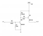
Make sure Q2 passes sufficient current to saturate Q1, when you require the Vcc to be turned to ON.
That prompts a couple of questions:
a.) what is the maximum current demand @ OUT ?
b.) what is the voltage drop across R3 when Q2 tells Q1 to pass that maximum demand?
That prompts a couple of questions:
a.) what is the maximum current demand @ OUT ?
b.) what is the voltage drop across R3 when Q2 tells Q1 to pass that maximum demand?
Demand? Good question. One green LED, a SG3525 controller, and two IRF3205 gates at 65khz each (push pull, 130khz oscillator frequency).
Here's some condition measurements from the sim (attached). I have the completed supply running behind me now. It's been on all day. Neither Q1 or Q2 show any significant heat. I'll try and get an actual current measurement off the Q1 collector later today. Voltage across R3 is 13.078v
I did have significant heating of my switching fets yesterday. I miscalculated Rt/Ct and had the oscillator at 60khz. I believe my transformer was saturating. It's ok at 130khz with slight heating of the ferrite. Nothing unmanageable. 42c at the moment.
Attachments

Last edited:
Vr3=13.078V
Vceq2~0.2V
Vbeq1=14-Vr3-Vceq2= 14-13.078-0.2=0.722V
Ibq1~13mA
Ieq1max ~10*Ibq1=~130mA
Why do you need a medium power device?
If maximum demand can exceed 130mApk, then you need to change R3 value.
Vceq2~0.2V
Vbeq1=14-Vr3-Vceq2= 14-13.078-0.2=0.722V
Ibq1~13mA
Ieq1max ~10*Ibq1=~130mA
Why do you need a medium power device?
Use another 500mA device.Need TO126 or TO225 package.
If maximum demand can exceed 130mApk, then you need to change R3 value.
Last edited:
I used what I had on hand. Board layout was for a TO126 and I have many BD139 and BD140 transistors. I'm open to other suggestions. Device selection is something I'm not good at. It's been easier for me to design around what I have on hand. Looking for a specific set of parameters is like finding a diamond in the desert. BD438 maybe? More gain, more current. Looking at the BD438 I may pick up a few for a small amp project.
Is 1k insufficient for base current? 13ma should be enough.
Is 1k insufficient for base current? 13ma should be enough.
Power mosfets in TO-220 etc are gds as the drain is the body of the die and connected to the tabTry a mosfet -- board was probably designed for this. they are DGS (except Renesas Lateral MOSFETS) so you'll have to rotate 180 degrees....
Hey, are you designing your own PCB? 🙂Ok thanks for the info. I'll try and work around a ECB pinout but it's not going to be fun.
No big deal, just reroute 2 tracks and *if* you painted yourself into a corner (not enough space to cross paths) , route one normally and add one wire jumper for the other so they cross without touching.
You don't really have a problem if you can solve it in 5 minutes. 😀
And as said before, plastic power packages place Collector in the middle, so it aligns with the metallic back plate for proper heatsinking.
As a general rule it's wise to design for regular components, for ease of sourcing and future maintenance.
Power mosfets in TO-220 etc are gds as the drain is the body of the die and connected to the tab
Current doesn't justify a mosfet.
Hey, are you designing your own PCB? 🙂
No big deal, just reroute 2 tracks and *if* you painted yourself into a corner (not enough space to cross paths) , route one normally and add one wire jumper for the other so they cross without touching.
You don't really have a problem if you can solve it in 5 minutes. 😀
And as said before, plastic power packages place Collector in the middle, so it aligns with the metallic back plate for proper heatsinking.
As a general rule it's wise to design for regular components, for ease of sourcing and future maintenance.
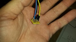
I was able to nudge some of the other components around to make room for the trace to get around the transistor for an ECB pinout. I had the board designed for an NPN switch (to turn on VCC) but it was causing an issue with another part of the circuit (long story). I removed the NPN and it's accompanying components and built the NPN/PNP circuit (posted above) on a small board that hangs off the main PCB. It seems to work quite well so I revised the design so they can be moved to the main PCB. I haven't had those printed yet.
Attachments
The switcher has to run saturated..
Is 1k insufficient for base current? 13ma should be enough.
i.e. Ie:Ib ~ 10:1
- Status
- Not open for further replies.
- Home
- Amplifiers
- Solid State
- Help finding a transistor with EBC pinout.