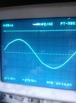
I tried to make a new amp, since the other one I made failed miserably, and I was thinking if someone here could help me identify the reason for the distortion seen on the picture below.
The amp is clocked (500kHz) and feedback is before the output filter. Filtered feedback signal looks ok, but the signal after the error amplifier looks like the output.
Dead time is set to 15n.
square waves at the gates and drain of the MOSFETs look good, with just a little bit of ringing, without load.
This distortion seems to start at medium output power, and at low frequencies is less evident.
I think it might be the feedback compensation, but I re-calculated everything and I believe it´s right...
I changed output inductors for other ones with the same value, the ICE 1D14A, can´t see a diference, but sounds better.
Attachments
Yeah, I´m sorry, but already solve the problem, it was the load I was using.
I connected some good speakers and its all good.
I think there´s a little to much bass, but still good for my first "working" class D amp.
I connected some good speakers and its all good.
I think there´s a little to much bass, but still good for my first "working" class D amp.
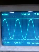
I didn´t have any 4 ohm resistor to test to amplifier, so I got one of those nickel chromium wires, I think, that are used to produce heat.
If this kind of load can induce distortion, then the amplifier doesn't work properly, unless resistance is too low.
What test did you do after, with what kind of speaker?
What test did you do after, with what kind of speaker?
I did the test again with the nickel wire. With low output power the signal looks normal, once I reach more less medium power the distortion appears.
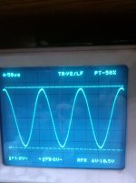
Also tested with the speaker (I used some MB Quart DCE 116 I got for free at a local shop) and apparently it´s not clean, as you can see in the picture there´s still something there, but way better compared to the wire.
I compared the sound of this amplifier against my Sony TA-F210.
And It sounded bad, so much punch I could not hear anything else. Changed the output inductor and increased the cutoff frequency, sooooo much better, still a bit muffled and reverbs are a little hard to notice.
Attachments
So there´s the schematic, it´s pretty basic.
I don´t know if it´s normal, but at almost full power, the voltage across the lower MOSFET´s overshoots 10V above the supply voltage which is 19V, seems high to me. Then I put some snubbers and it decreased a little, about 2 or 3V.
The ground lead is connected to the amp ground, used 2 probes to measure the output.
Attachments
Last edited:
L1 = L2?
yes, there was a little error, they are both 10uH.
So there´s the schematic, it´s pretty basic.
I don´t know if it´s normal, but at almost full power, the voltage across the lower MOSFET´s overshoots 10V above the supply voltage which is 19V, seems high to me. Then I put some snubbers and it decreased a little, about 2 or 3V.
The ground lead is connected to the amp ground, used 2 probes to measure the output.
There are some serious error in schematic.
1: Triangle generator is wrong, R1, R2 swapped.
2: U3A negative feedback is not connected. OK, maybe this is only in the drawing.
3: Even if it was connected correctly, the voltage ranges are not matched. At zero output voltage on bridge, the difference amplifier gives 0 voltage. But what about negative output voltage? OPA can not give negative voltage, since fed from single rail!
Maybe your feedback doesn't work at all. At least not as the schematic shows. Reference of U2A and U3A must be the same (2.5V)! This reference must be absolutely free from audible noise. 5 V is not that important, but must be relatively clean also, especially at high freq.
Otherwise not a bad design.
Last edited:
There are some serious error in schematic.
1: Triangle generator is wrong, R1, R2 swapped.
2: U3A negative feedback is not connected. OK, maybe this is only in the drawing.
3: Even if it was connected correctly, the voltage ranges are not matched. At zero output voltage on bridge, the difference amplifier gives 0 voltage. But what about negative output voltage? OPA can not give negative voltage, since fed from single rail!
Maybe your feedback doesn't work at all. At least not as the schematic shows. Reference of U2A and U3A must be the same (2.5V)! This reference must be absolutely free from audible noise. 5 V is not that important, but must be relatively clean also, especially at high freq.
Otherwise not a bad design.
yes, the schematic is wrong... sorry.
the oscilator resistors are swapped.
the 1k resistor and 4.7n capacitor , in U3A, aren´t connected to ground but to the 2.5V reference.
I see in the scope about 50mV peak noise( high frequency), both in the 5V and 2.5V rails, at full power.
Attachments
Last edited:
Negative feedback is still missing, but I think it's there in reality.
50 mV is not tragically high, but can be a sign of not proper GND plane.
Gate discharge could have been faster, maybe cross conduction is the reason for the overshoot on drains.
Your control loop can be good in theory, but in practice maybe a little too fast. I didn't check in detail. Also maybe U3A OPA can't handle perfectly the transients.
If you don't need high rail voltage, it's better to use MOSFETs with lower Vds voltage.
Negative feedback is still missing, but I think it's there in reality.
50 mV is not tragically high, but can be a sign of not proper GND plane.
Gate discharge could have been faster, maybe cross conduction is the reason for the overshoot on drains.
Your control loop can be good in theory, but in practice maybe a little too fast. I didn't check in detail. Also maybe U3A OPA can't handle perfectly the transients.
If you don't need high rail voltage, it's better to use MOSFETs with lower Vds voltage.
Removed the turn off resistor in the gate and peaks got bigger.
Increased dead-time and still the same high peaks, so I guess it´s not cross conduction, but to much stray inductance.
Still have not reduced the loop response time, but I´m really thinking it´s the PCB.
I used two ground planes connected to a single point, but they have a lot of traces through.
Anyway, thanks Pafi.
- Status
- Not open for further replies.
- Home
- Amplifiers
- Class D
- Help, distortion!!