Hi, I'm working on designing a small class D mono amp for a portable radio project. The current design is based on a number of other projects, so I need some clarification and advice.
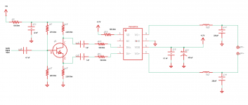
The audio signal is amplified and converted to differential signals using a BJT NPN transistor as a Class A amplifier. the Vcc is a fixed 3v. The signal is then amplified by a small class D amplifier chip (PAM8302) which is powered by a single li-ion cell, so the voltage ranges between 3.5 and 4.2V.
My main questions:
Thanks for the help and advice!
The audio signal is amplified and converted to differential signals using a BJT NPN transistor as a Class A amplifier. the Vcc is a fixed 3v. The signal is then amplified by a small class D amplifier chip (PAM8302) which is powered by a single li-ion cell, so the voltage ranges between 3.5 and 4.2V.
My main questions:
- I'm using a 4.7 uF ceramic input cap for the NPN transistor. Is that an appropriate value?
- The output caps are 1 uF ceramic. I know those caps set a high pass filter and I think they need to be larger to ensure good low end response (ideally 40 Hz), but I'm not sure how to calculate the necessary value. Can I use a large electrolytic cap instead of ceramic?
- I'm using two bypass caps for the supply input on the class D amp; one small ceramic and one 470 uF electrolytic. Will this work for accurate low end response?
Thanks for the help and advice!
Attachments
The npn-phase inverter will not work due to wrong biasing.
I recommend testing this with LTSpice.
Polarity of coupling caps should be checked anyway.
I recommend testing this with LTSpice.
Polarity of coupling caps should be checked anyway.
Bucks bunny,
Assuming the hFE (DC value) of the BJT is high, the biasing resistors are in such a way that most of the current entering the circuit from the top resistor needs to return through the bottom one, leaving only a small portion which flows into the transistor as base current. This usually gives values that are close to each other, like 27k, 22k as used by the OP. The small signal gain (Rc/Re) is unity which is also correct, considering the negligible base current.
Bcschmi,
* The input impedance of your biasing network is approximately 27k//22k = 12k. With a 4.7uF coupling capacitor, your lower cutoff frequency should be around 1/2*pi*4.7u*12k = 3 Hz, which is just about right for an amplifier.
* The output highpass corner may also be calculated as above using the differential input impedance of the next (class d) stage as 16Hz.
* The 470uF + ceramic decoupling should be sufficient, given the small power of the application and bridge tied load.
All the best.
Thank you for all the help! So the schematic as is would work well for a small portable speaker and have accurate response down to about 100 Hz?
I do not see gross mistakes. If you want to route your pcb you should study layout considerations from the manufacturer.Thank you for all the help! So the schematic as is would work well for a small portable speaker and have accurate response down to about 100 Hz?
I have some more questions to better understand the transistor amplification part of the schematic:
- Would the collector current be around 0.7 ma? I'm using the formula Rc = VCC/Ic x 2, with an Rc value of 2.2K ohms.
- If the emitter drops 10% of the supply voltage, shouldn't the emitter resistor value be Ve/Ie = 428 ohms? Why does this schematic use the same values for Rc and Re?
Being a phase inverter, Vce = Vcc/2 and Vr-low = Vr-hi = Vcc/4, thus summing up to Vcc. Simulate the circuitry with LTSpice and you will see how it works.I have some more questions to better understand the transistor amplification part of the schematic:
- Would the collector current be around 0.7 ma? I'm using the formula Rc = VCC/Ic x 2, with an Rc value of 2.2K ohms.
- If the emitter drops 10% of the supply voltage, shouldn't the emitter resistor value be Ve/Ie = 428 ohms? Why does this schematic use the same values for Rc and Re?
- Home
- Amplifiers
- Class D
- Help designing a small Class D amp