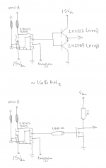
I have constructed a simple PWM amplifier based on two CMOS 555 timers that happily puts out tidy little square waves in the 160 KHz region. I have successfully buffered this amplifier with the complementary symmetry output stage depicted in the first drawing — but without a redesign, I am limited to running the output stage at the maximum voltage the 555 will tolerate (somewhere south of 18 volts) since the output swing is only as big as the input signal.
My understanding is that the two ways to increase power into the load (just the scope at the moment) are to increase the degree to which the signal is modulating the duty cycle and to increase the voltage of the pulses. This is where I am stuck.
I have tried a variant of the first drawing that inserts another 2n2222 configured as a voltage amplifier between the timer and the buffer stage. I have found that the lower the load resistor, the squarer the wave at the output of the voltage amplifier (1k still looks pretty good on the scope).
With this setup, I can use a "high" voltage power supply for the voltage amplifier and the output stage and a "low" voltage for the timer. The problem is that anything past 18 volts tends to release the magic smoke from all three transistors. With no appreciable load (just the scope), I am unsure why this would be the case. The only beefier complementary transistor pairs I have are Darlingtons, and my understanding is that they are too slow for this application.
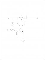
I have tried using a single-ended MOSFET voltage amplifier (as depicted in the second picture) as an output stage, but the load resistor has to be a pretty small value to keep the wave square – and my ultimate goal is portability/efficiency.
Without totally reinventing the wheel, I'd love to bring the switched output up to about forty volts. Any thoughts would be greatly appreciated.
My understanding is that the two ways to increase power into the load (just the scope at the moment) are to increase the degree to which the signal is modulating the duty cycle and to increase the voltage of the pulses. This is where I am stuck.
I have tried a variant of the first drawing that inserts another 2n2222 configured as a voltage amplifier between the timer and the buffer stage. I have found that the lower the load resistor, the squarer the wave at the output of the voltage amplifier (1k still looks pretty good on the scope).
With this setup, I can use a "high" voltage power supply for the voltage amplifier and the output stage and a "low" voltage for the timer. The problem is that anything past 18 volts tends to release the magic smoke from all three transistors. With no appreciable load (just the scope), I am unsure why this would be the case. The only beefier complementary transistor pairs I have are Darlingtons, and my understanding is that they are too slow for this application.
I have tried using a single-ended MOSFET voltage amplifier (as depicted in the second picture) as an output stage, but the load resistor has to be a pretty small value to keep the wave square – and my ultimate goal is portability/efficiency.
Without totally reinventing the wheel, I'd love to bring the switched output up to about forty volts. Any thoughts would be greatly appreciated.
Attachments
Hi,
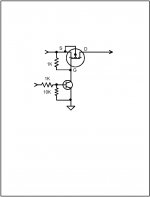
The problem it is that you are grounding the output signal and that will damage the transistor. Why not you just feed the base of the transistor or the mosfet. and let the emitter drive the load. Normally I used 1K resistor to drive the transistor and then use a 10K from the base to ground. The 10K resistor it is use to discharge the base.
The problem it is that you are grounding the output signal and that will damage the transistor. Why not you just feed the base of the transistor or the mosfet. and let the emitter drive the load. Normally I used 1K resistor to drive the transistor and then use a 10K from the base to ground. The 10K resistor it is use to discharge the base.
Tauro,
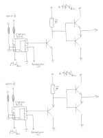
Thank you for the prompt response. If I am reading your response correctly, it sounds like you are suggesting that I add an emitter follower between the 555 and the class B output stage. Unless I am missing something, this doesn't solve my problem because the emitter follower configuration has a gain figure that is slightly less than unity. On the attached graphic, the top figure represents the circuit with the voltage amplifier section that likes to self-destruct. The bottom figure (using a PNP transistor) represents what I believe you are suggesting.
Thank you for the prompt response. If I am reading your response correctly, it sounds like you are suggesting that I add an emitter follower between the 555 and the class B output stage. Unless I am missing something, this doesn't solve my problem because the emitter follower configuration has a gain figure that is slightly less than unity. On the attached graphic, the top figure represents the circuit with the voltage amplifier section that likes to self-destruct. The bottom figure (using a PNP transistor) represents what I believe you are suggesting.
Attachments
- Status
- Not open for further replies.
- Home
- Amplifiers
- Class D
- Help Adding an Output Stage to a 555-Based PWM Amplifier