So , I study Tom´s description of grounding.
Everything is now understanding.
But I thing Tom has in his text and description an error.
His text description do not fit with his picture.
He wrote :
"The only difference between the star ground and the improved grounding scheme is that the GND_SIG trace was routed to the output connector rather than to the star ground"
Thats not correct if I verify the used standard star and his better star connection....
There are one difference more:
His GND_LOAD goes not more direct to earth GND , it goes over GND Power.
So the text is in my opinion not fitting to his picture.
??? what are you thinking ???
??? what are you thinking ???
Have I understand something wrong or is there really an text missunderstanding.
Please have a look to the picture and the text and help my understanding what tom mean .
kind regards
Have I understand something wrong or is there really an text missunderstanding.
Please have a look to the picture and the text and help my understanding what tom mean .
kind regards
I think you will get more help if you show us your complete pcb layout.
I also cannot find any "earth ground" in tom's text ...
Please also take into considerstion that it may not be so important to make the perfect pcb if this is only a test and learning project. Try to understand all information you can find. This will take some time!
And one more hint: don't open new threads for every new question. Just add them here!
hmm, i learned in other forums, each topis should be as one theme 🙂 Thats why i do so.I think you will get more help if you show us your complete pcb layout.
I also cannot find any "earth ground" in tom's text ...
Please also take into considerstion that it may not be so important to make the perfect pcb if this is only a test and learning project. Try to understand all information you can find. This will take some time!
And one more hint: don't open new threads for every new question. Just add them here!
On the other side , i learned , that not all go in that topic, because the titel do not fit what later comes
on questions....
Sure showing the complete layout and shematic is good, but then i think , all discuss about all.
And this do not help me, so i think its better to conctrate to my questions by Part.
100% become discussuins about stuff in do not ask 🙂 🙂
So only the parts 🙂
And a 3 point, I want to do my own experience in most parts.
So I ask only what is not clear for me...
Then I have a real own made board.
I there comes 100 hints what I make wrong, then its not more by me.
So my way... Understand what i can understand ... make what I think is good.
Ask what is not clear and get help... but only this...
Then think about that and try to understand and then used it or modify it.
Selfmade by Teeny 🙂
Can you understand my way a little bit... and if I make bu*shi**, then I see it 🙂 a do the
research again.
And last but not least, we have in the near an EMI laboraty, I ask them about a THD Measurement.
Fine people... I can come 2-3 times in the break of them and they make these with my, but I must support them
by backing cakes 🙂
..." to make the perfect pcb if this is only a test and learning project"
Yes, you are right, but if the playboard has a good start condition is was perfect.
Yes learning take some time, but now i thing must come the practical part for measuring.
I have one board from Amazon , from China... Worst!
LM3886 Fakes on it with NS logo...! Real LM3886 comes first end of Feb and are very rar!
A FAE confirm, that my LM3886 is a fake by verify my pictures.
I know a FAE because last year I do some for "youth researches" in Germany.
Last edited:
But grounding and dc servo for lm3886 are still subject to "🙂 🙂 🙂 * Hello diyAudio members, I need some help in many questions about LM3886 * 🙂 🙂 🙂"
Don't be shy with your layout, if you want best help you should provide the best basis!
Don't be shy with your layout, if you want best help you should provide the best basis!
So one a last for today.
I make my own GND Playboard.
I Make all 4 Gnds seperate , but so that i can decide on Bottom of PCB By SMD metall bridge 0 OHM which is
better, the classic star ground or that what Tom show in his pictures, not the text.
SO in my 1 innerlayer are over Bottom and R field all configurations possible.
Thinkig Audio GND goes not to star, but it is prepared to test w and wo.
Attachments
Last edited:
Use a braided shield wire to connect grounds if needed, it can carry less induced currents I think.
jup and power , only twisted at higher currents....so 0V and -25V twisted and +25V and 0V twisted, also 🙂Use a braided shield wire to connect grounds if needed, it can carry less induced currents I think.
No joke you see in jumping currents the effect of twisted power cables 🙂
ok, now I undertand you meaned the flat cupper braided EMI wires.. I know them, thanks!I meant use shield wire from PCB grounds to chassis grounds
Yes of course !
Hi everybody,
meanwhile I received my PCBs andf i start the testing.
First it do not work and I looking for the reasons.
I found out very fast what do not work.
Now, everthing is fine and works.
But for one point I need help and a explanation.
First it do not works, because the composite OPV works on
(look like) infinite gain and put out a square wave insteadt of the 1kHz Sinus.
I have here at first 47pF.
After using a 100nF it works fine with the caculated gain of r.a. 20.
But I see that if i take for example up to 4,7µF then the Gain goes down.
Please keep in your mind that the Rs of 20k and 1k always stay on their place.
By changig the Value of "C composite" I get this results.
0,1 µF ~ Gain 20
1µf ~ Gain 12
4,7µF ~ Gain 10
Can anybody please explain me the
function and mode of action of the C on the composite OPV ?
Please see a short simplified sketch attached.
Attachments
this cap acts as local feedback for the op-amp and makes a low pass filter out of it. the cap will turn the op-amp in a simple voltage follower for frequencies depending on the value of the cap.Can anybody please explain me the
function and mode of action of the C on the composite OPV ?
this cap is to stabilize the circuit for high frequencies (avoiding oscillation), as far as i understand it.
I suppose your amp is not working (stable) yet.
but by heavily reducing the bandwidth/gain of the op-amp with the huge caps you get it to work, somehow.
i suggest you simulate the circuit to see what is happening (simulate only the op-amp with cap first).
you will see that all caps you selected severely limit the bandwith of the op-amp and thus also limit the "composite" correcting function of it.
(anyhow, this is just my very simplistic view - i'm no expert in this!)
here is the frequency response for the complete amp with 0,1 uF and 4,7 uF opamp-feedback-cap.
you need to add 20 dB for actual gain, because i simulated with 0,1 V input!
i did not have all values, so it might be slightly different yet.
I also do not think the 100 uF cap in the local LM feedback loop makes much sense. the composite amp will be corrected by the op-amp anyways.
I still think you should either get deeper knowledge about composite amps or build a simple non-composite amp with your LM3886.
Attachments

Dear STV,here is the frequency response for the complete amp with 0,1 uF and 4,7 uF opamp-feedback-cap.
you need to add 20 dB for actual gain, because i simulated with 0,1 V input!
i did not have all values, so it might be slightly different yet.
I also do not think the 100 uF cap in the local LM feedback loop makes much sense. the composite amp will be corrected by the op-amp anyways.
I still think you should either get deeper knowledge about composite amps or build a simple non-composite amp with your LM3886.
many thanks for these answer and your Text.
Yes, i begin to understand, slowly. Of course I better go deeper in composite mode.
I see, it is not so easy as i think first.
Ok, lerning by doing.
StV, would you share the Spice File with me please m, is this possible.
And again, Thanks for your explanation.
kind regards
Michaela
so one last question.this cap acts as local feedback for the op-amp and makes a low pass filter out of it. the cap will turn the op-amp in a simple voltage follower for frequencies depending on the value of the cap.
this cap is to stabilize the circuit for high frequencies (avoiding oscillation), as far as i understand it.
I suppose your amp is not working (stable) yet.
but by heavily reducing the bandwidth/gain of the op-amp with the huge caps you get it to work, somehow.
i suggest you simulate the circuit to see what is happening (simulate only the op-amp with cap first).
you will see that all caps you selected severely limit the bandwith of the op-amp and thus also limit the "composite" correcting function of it.
(anyhow, this is just my very simplistic view - i'm no expert in this!)
In Theorie, if all was perfect, design,layout and all are ideal, so it must work also without the C ?
Meanwhile i found out what make the instability, i have chosen the wrong GNDs for the Feebacks Rs.
I take them to the GND which was for the OPA and Signal
After switch the Feedbacks Rs to Power GND it works with only 470pf , but now it was manuellay modified.
I think in a second PCB I come to 47pf down, because i see with light load now 47pf is also working now.
Also the gain fits now.
.... step by step...
hi micha,
attached the spice file.
please note:
that's an extremely simplified model with "ideal op-amps" just to show the influence of the first op-amp feedback cap.
input signal is 0,1 V. however, spice refers the dB scale to 1 V. that's why input is -20 dB and output is around 12 dB (for low frequencies, for a total gain of ~32 dB).
have fun!
stv
Attachments
I don't think so - it would probably oscillate.so it must work also without the C
but you need to dig deeper into this matter - it's not that simple.
there are plenty of threads here dealing with similar projects, just type "composite amp" into the search field.
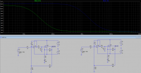
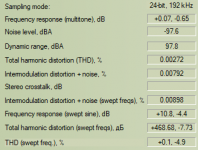
Hi all,
meantime I made a redesign with all I see so and learnd.
And , of course it is possible to go down with the Cff to 4,7pF 🙂 ... now yes 🙂
What are you thinking about this results:
LM3886 in Composite Mode and unbalanced 2 Wire input.
The instrumental Amps are in this measurent not in action ( this later for the XLR connectors), because I do not solder them today.
Are this good results for my second Board ?
Is this a good or worse result for a composite board in 4 layer ?
The results are based on 20Vpp Out and 4 Ohm load and 2Vpp input.
Crostalk is not in use, because I solder first one board.
kind regards
Micha
Attachments
This "composite amplifier" is perhaps a bad idea. It attempts to improve the distortion performance of the LM3886 by adding additional feedback. But there is a limit to the amount of feedback that can be applied to any circuit before it oscillates. This is because any amplifier has a delay and increasing phase shift as the frequency increases. At some frequency the phase shift changes the negative feedback into positive feedback, 180 degrees shift, and positive feedback is the reason a circuit oscillates, as soon as that feedback exceeds unity gain, ie enough to recreate itself. You will find many articles on feedback stability on the internet, but most use complicated mathematics to precisely define it. This does not help beginners understand the simple idea. An important concept is that many small delays, aka high frequency "poles" each add significant amount of phase shift but not much attenuation resulting is a lot of positive feedback. So, a single dominant pole, ie at a much lower frequency than the others, has a maximum phase shift of 90 degrees but continues to attenuate at 1/frequency, so the feedback is reduced below unity before an addition 90 degrees of phase shift from other poles makes it dangerous. The stability of an amplifier can be predicted is spice using a feedback probe and plotting the loop gain vs phase. See DIYA posts about the "Tian probe", again, over complicating a simple idea. LTC spice includes feedback probes in their sample circuits.
The LM3886 and most operational amplifies usually contain "internal compensation" which means that they have a dominant pole built in that makes them feedback stable for unity gain feedback, usually a ~30pF capacitator on the VAS (voltage amplifier stage). But when you add additional gain, they are no longer stable. Many audio amplifier chips are not unity gain stable because it is assumed that they will be used with a gain of at least 5x or 10x, and compensating them for unity gain would make them unnecessarily slow, i.e. poor high frequency response and "slew limited".
Feedback stability is a complicated subject, and I could talk more about it but I think this is enough for now.
Last edited:
- Home
- Amplifiers
- Chip Amps
- :-) :-) :-) *** Hello diyAudio members, I need some help in many questions about LM3886 *** :-) :-) :-)